
Datasheet
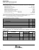


SN74AHCT1G00
SINGLE 2-INPUT POSITIVE-NAND GATE
SCLS316M – MARCH 1996 – REVISED JANUARY 2003
1
POST OFFICE BOX 655303 • DALLAS, TEXAS 75265
Operating Range of 4.5 V to 5.5 V
Max t
pd
of 7.1 ns at 5 V
Low Power Consumption, 10-µA Max I
CC
±8-mA Output Drive at 5 V
Inputs Are TTL-Voltage Compatible
Latch-Up Performance Exceeds 250 mA Per
JESD 17
ESD Protection Exceeds JESD 22
– 2000-V Human-Body Model (A114-A)
– 200-V Machine Model (A115-A)
– 1000-V Charged-Device Model (C101)
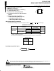
description/ordering information
The SN74AHCT1G00 performs the Boolean function Y = A • B or Y = A + B in positive logic.
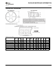
ORDERING INFORMATION
T
A
PACKAGE
†
ORDERABLE
PART NUMBER
TOP-SIDE
MARKING
‡
SOT (SOT 23) DBV
Reel of 3000 SN74AHCT1G00DBVR
B00
40°Cto85°C
SOT
(SOT
-
23)
–
DBV
Reel of 250 SN74AHCT1G00DBVT
B00
_
–
40°C
t
o
85°C
SOT (SC 70) DCK
Reel of 3000 SN74AHCT1G00DCKR
BA
SOT
(SC
-
70)
–
DCK
Reel of 250 SN74AHCT1G00DCKT
BA
_
†
Package drawings, standard packing quantities, thermal data, symbolization, and PCB design guidelines are
available at www.ti.com/sc/package.
‡
The actual top-side marking has one additional character that designates the assembly/test site.
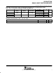
FUNCTION TABLE
INPUTS
OUTPUT
A B
Y
H H L
L XH
X L H
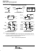
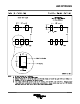
logic diagram (positive logic)
A
B
Y
1
2
4
DBV OR DCK PACKAGE
(TOP VIEW)
1
2
3
5
4
A
B
GND
V
CC
Y
PRODUCTION DATA information is current as of publication date.
Products conform to specifications per the terms of Texas Instruments
standard warranty. Production processing does not necessarily include
testing of all parameters.
Copyright 2003, Texas Instruments Incorporated
Please be aware that an important notice concerning availability, standard warranty, and use in critical applications of
Texas Instruments semiconductor products and disclaimers thereto appears at the end of this data sheet.