
Datasheet


SN54ALVTH162244, SN74ALVTH162244
2.5-V/3.3-V 16-BIT BUFFERS/DRIVERS
WITH 3-STATE OUTPUTS
SCES074E – JUNE 1996 - REVISED JANUARY 1999
2
POST OFFICE BOX 655303 • DALLAS, TEXAS 75265
description (continued)
These devices can be used as four 4-bit buffers, two 8-bit buffers, or one 16-bit buffer. These devices provide
true outputs and symmetrical active-low output-enable (OE
) inputs.
Active bus-hold circuitry is provided to hold unused or floating data inputs at a valid logic level.
When V
CC
is between 0 and 1.2 V, the device is in the high-impedance state during power up or power down.
However, to ensure the high-impedance state above 1.2 V, OE
should be tied to V
CC
through a pullup resistor;
the minimum value of the resistor is determined by the current-sinking capability of the driver.
All outputs are designed to sink up to 12 mA and include equivalent 30-Ω resistors to reduce overshoot and
undershoot.
The SN54ALVTH162244 is characterized for operation over the full military temperature range of –55°C to
125°C. The SN74ALVTH162244 is characterized for operation from –40°C to 85°C.
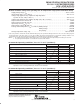
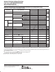
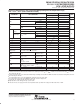
FUNCTION TABLE
(each 4-bit buffer)
INPUTS
OUTPUT
OE
A
Y
L H H
L LL
HXZ
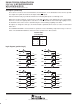
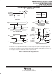
logic diagram (positive logic)
1OE
1A1
1A2
1A3
1A4
1Y1
1Y2
1Y3
1Y4
1
47
46
44
43
2
3
5
6
2OE
2A1
2A2
2A3
2A4
2Y1
2Y2
2Y3
2Y4
48
41
40
38
37
8
9
11
12
3OE
3A1
3A2
3A3
3A4
3Y1
3Y2
3Y3
3Y4
25
36
35
33
32
13
14
16
17
4OE
4A1
4A2
4A3
4A4
4Y1
4Y2
4Y3
4Y4
24
30
29
27
26
19
20
22
23