
Datasheet
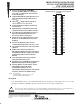
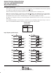


SN54ALVTH162244, SN74ALVTH162244
2.5-V/3.3-V 16-BIT BUFFERS/DRIVERS
WITH 3-STATE OUTPUTS
SCES074E – JUNE 1996 - REVISED JANUARY 1999
3
POST OFFICE BOX 655303 • DALLAS, TEXAS 75265
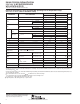
absolute maximum ratings over operating free-air temperature range (unless otherwise noted)
†
Supply voltage range, V
CC
–0.5 V to 4.6 V. . . . . . . . . . . . . . . . . . . . . . . . . . . . . . . . . . . . . . . . . . . . . . . . . . . . . . . . .
Input voltage range, V
I
(see Note 1) –0.5 V to 7 V. . . . . . . . . . . . . . . . . . . . . . . . . . . . . . . . . . . . . . . . . . . . . . . . . .
Voltage range applied to any output in
the high-impedance
or power-off state, V
O
(see Note 1) –0.5 V to 7 V. . . . . . . . . . . . . . . . . . . . . . . . . . . . . . . . . . . . . . . . . . . . . . . .
Voltage range applied to any output in the high state, V
O
(see Note 1) –0.5 V to 7 V. . . . . . . . . . . . . . . . . . . .
Output current in the low state, I
O
30 mA. . . . . . . . . . . . . . . . . . . . . . . . . . . . . . . . . . . . . . . . . . . . . . . . . . . . . . . . . .
Output current in the high state, I
O
–30 mA. . . . . . . . . . . . . . . . . . . . . . . . . . . . . . . . . . . . . . . . . . . . . . . . . . . . . . . .
Input clamp current, I
IK
(V
I
< 0) –50 mA. . . . . . . . . . . . . . . . . . . . . . . . . . . . . . . . . . . . . . . . . . . . . . . . . . . . . . . . . . .
Output clamp current, I
OK
(V
O
< 0) –50 mA. . . . . . . . . . . . . . . . . . . . . . . . . . . . . . . . . . . . . . . . . . . . . . . . . . . . . . . .
Package thermal impedance, θ
JA
(see Note 2): DGG package 89°C/W. . . . . . . . . . . . . . . . . . . . . . . . . . . . . . .
DGV package 93°C/W. . . . . . . . . . . . . . . . . . . . . . . . . . . . . . . .
DL package 94°C/W. . . . . . . . . . . . . . . . . . . . . . . . . . . . . . . . .
Storage temperature range, T
stg
–65°C to 150°C. . . . . . . . . . . . . . . . . . . . . . . . . . . . . . . . . . . . . . . . . . . . . . . . . . .
†
Stresses beyond those listed under “absolute maximum ratings” may cause permanent damage to the device. These are stress ratings only, and
functional operation of the device at these or any other conditions beyond those indicated under “recommended operating conditions” is not
implied. Exposure to absolute-maximum-rated conditions for extended periods may affect device reliability.
NOTES: 1. The input and output negative-voltage ratings may be exceeded if the input and output clamp-current ratings are observed.
2. The package thermal impedance is calculated in accordance with JESD 51.
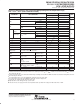
recommended operating conditions, V
CC
= 2.5 V ± 0.2 V (see Note 3)
SN54ALVTH162244 SN74ALVTH162244
UNIT
MIN TYP MAX MIN TYP MAX
UNIT
V
CC
Supply voltage 2.3 2.7 2.3 2.7 V
V
IH
High-level input voltage 1.7 1.7 V
V
IL
Low-level input voltage 0.7 0.7 V
V
I
Input voltage 0 V
CC
5.5 0 V
CC
5.5 V
I
OH
High-level output current –6 –8 mA
I
OL
Low-level output current 8 12 mA
∆t/∆v Input transition rise or fall rate Outputs enabled 10 10 ns/V
∆t/∆V
CC
Power-up ramp rate 200 200 µs/V
T
A
Operating free-air temperature –55 125 –40 85 °C
NOTE 3: All unused control inputs of the device must be held at V
CC
or GND to ensure proper device operation. Refer to the TI application report,
Implications of Slow or Floating CMOS Inputs
, literature number SCBA004.
recommended operating conditions, V
CC
= 3.3 V ± 0.3 V (see Note 3)
SN54ALVTH162244 SN74ALVTH162244
UNIT
MIN TYP MAX MIN TYP MAX
UNIT
V
CC
Supply voltage 3 3.6 3 3.6 V
V
IH
High-level input voltage 2 2 V
V
IL
Low-level input voltage 0.8 0.8 V
V
I
Input voltage 0 V
CC
5.5 0 V
CC
5.5 V
I
OH
High-level output current –8 –12 mA
I
OL
Low-level output current 8 12 mA
∆t/∆v Input transition rise or fall rate Outputs enabled 10 10 ns/V
∆t/∆V
CC
Power-up ramp rate 200 200 µs/V
T
A
Operating free-air temperature –55 125 –40 85 °C
NOTE 3: All unused control inputs of the device must be held at V
CC
or GND to ensure proper device operation. Refer to the TI application report,
Implications of Slow or Floating CMOS Inputs
, literature number SCBA004.
PRODUCT PREVIEW information concerns products in the formative or
design phase of development. Characteristic data and other
specifications are design goals. Texas Instruments reserves the right to
change or discontinue these products without notice.