
Datasheet
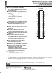


SN54ALVTH162244, SN74ALVTH162244
2.5-V/3.3-V 16-BIT BUFFERS/DRIVERS
WITH 3-STATE OUTPUTS
SCES074E – JUNE 1996 - REVISED JANUARY 1999
5
POST OFFICE BOX 655303 • DALLAS, TEXAS 75265
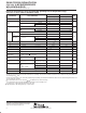
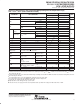
electrical characteristics over recommended operating free-air temperature range,
V
CC
= 3.3 V ± 0.3 V (unless otherwise noted)
PARAMETER
TEST CONDITIONS
SN54ALVTH162244 SN74ALVTH162244
UNIT
PARAMETER
TEST
CONDITIONS
MIN TYP
†
MAX MIN TYP
†
MAX
UNIT
V
IK
V
CC
= 3 V, I
I
= –18 mA –1.2 –1.2 V
V
CC
= 3 V to 3.6 V, I
OH
= –100 µA V
CC
–0.2 V
CC
–0.2
V
OH
V
CC
=3V
I
OH
= –8 mA 2
V
V
CC
=
3
V
I
OH
= –12 mA 2
V
CC
= 3 V to 3.6 V, I
OL
= 100 µA 0.2 0.2
V
OL
V
CC
=3V
I
OL
= 8 mA 0.8
V
V
CC
=
3
V
I
OL
= 12 mA 0.8
Control
V
CC
= 3.6 V, V
I
= V
CC
or GND ±1 ±1
inputs
V
CC
= 0 or 3.6 V V
I
= 5.5 V 10 10
I
I
V
I
= 5.5 V 10 10
µA
Data inputs V
CC
= 3.6 V
V
I
= V
CC
1 1
V
I
= 0 –5 –5
I
off
V
CC
= 0, V
I
or V
O
= 0 to 4.5 V ±100 µA
I
BHL
‡
V
CC
= 3 V, V
I
= 0.8 V 75 75 µA
I
BHH
§
V
CC
= 3 V, V
I
= 2 V –75 –75 µA
I
BHLO
¶
V
CC
= 3.6 V, V
I
= 0 to V
CC
500 500 µA
I
BHHO
#
V
CC
= 3.6 V, V
I
= 0 to V
CC
–500 –500 µA
I
EX
||
V
CC
= 3 V, V
O
= 5.5 V 125 125 µA
I
OZ(PU/PD)
V
CC
≤ 1.2 V, V
O
= 0.5 V to V
CC
,
V
I
= GND or V
CC
, OE
= don’t care
±100 ±100 µA
I
OZH
V
CC
= 3.6 V
V
O
= 3 V,
V
I
= 0.8 V or 2 V
5 5 µA
I
OZL
V
CC
= 3.6 V
V
O
= 0.5 V,
V
I
= 0.8 V or 2 V
–5 –5 µA
V
CC
=
3.6 V,
Outputs high 0.07 0.1 0.07 0.1
I
CC
V
CC
=
3
.
6
V
,
I
O
= 0,
Outputs low 3.2 5 3.2 5
mA
V
I
= V
CC
or GND
Outputs disabled 0.07 0.1 0.07 0.1
∆I
CC
V
CC
= 3 V to 3.6 V, One input at V
CC
– 0.6 V,
Other inputs at V
CC
or GND
0.4 0.4 mA
C
i
V
CC
= 3.3 V, V
I
= 3.3 V or 0 3 3 pF
C
o
V
CC
= 3.3 V, V
O
= 3.3 V or 0 6 6 pF
†
All typical values are at V
CC
= 3.3 V, T
A
= 25°C.
‡
The bus-hold circuit can sink at least the minimum low sustaining current at V
IL
max. I
BHL
should be measured after lowering V
IN
to GND and
then raising it to V
IL
max.
§
The bus-hold circuit can source at least the minimum high sustaining current at V
IH
min. I
BHH
should be measured after raising V
IN
to V
CC
and
then lowering it to V
IH
min.
¶
An external driver must source at least I
BHLO
to switch this node from low to high.
#
An external driver must sink at least I
BHHO
to switch this node from high to low.
||
Current into an output in the high state when V
O
> V
CC
High-impedance state during power up or power down
This is the increase in supply current for each input that is at the specified TTL voltage level rather than V
CC
or GND.
PRODUCT PREVIEW information concerns products in the formative or
design phase of development. Characteristic data and other
specifications are design goals. Texas Instruments reserves the right to
change or discontinue these products without notice.