
Datasheet


SDAS187A − APRIL 1982 − REVISED DECEMBER 1994
Copyright 1994, Texas Instruments Incorporated
1
POST OFFICE BOX 655303 • DALLAS, TEXAS 75265
POST OFFICE BOX 1443 • HOUSTON, TEXAS 77251−1443
• Package Options Include Plastic
Small-Outline (D) Packages, Ceramic Chip
Carriers (FK), and Standard Plastic (N) and
Ceramic (J) 300-mil DIPs
description
These devices contain four independent 2-input
positive-NAND gates. They perform the Boolean
functions Y = A
• B or Y = A + B in positive logic.
The SN54ALS00A and SN54AS00 are
characterized for operation over the full military
temperature range of −55°C to 125°C. The
SN74ALS00A and SN74AS00 are characterized
for operation from 0°C to 70°C.
FUNCTION TABLE
(each gate)
INPUTS
OUTPUT
A B
OUTPUT
Y
H H L
L XH
X L H
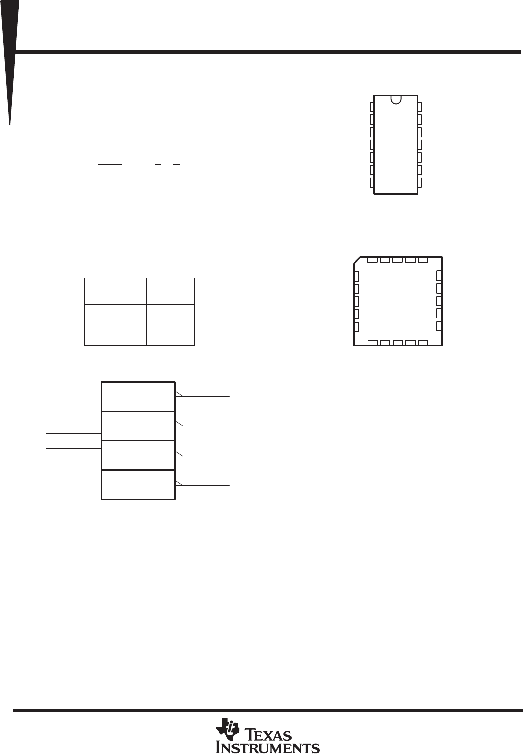
logic symbol
†
1
1A
2
1B
4
2A
5
2B
9
3A
10
3B
12
4A
13
4B
&
1Y
3
2Y
6
3Y
8
4Y
11
†
This symbol is in accordance with ANSI/IEEE Std 91-1984 and
IEC Publication 617-12.
Pin numbers shown are for the D, J, and N packages.
SN54ALS00A, SN54AS00 ...J PACKAGE
SN74ALS00A, SN74AS00 ...D OR N PACKAGE
(TOP VIEW)
1
2
3
4
5
6
7
14
13
12
11
10
9
8
1A
1B
1Y
2A
2B
2Y
GND
V
CC
4B
4A
4Y
3B
3A
3Y
SN54ALS00A, SN54AS00 . . . FK PACKAGE
(TOP VIEW)
3 2 1 20 19
9 10 11 12 13
4
5
6
7
8
18
17
16
15
14
4A
NC
4Y
NC
3B
1Y
NC
2A
NC
2B
1B
1A
NC
3Y
3A
V
4B
2Y
NC
CC
NC − No internal connection
GND
! " #$%! " &$'(#! )!%*
)$#!" # ! "&%##!" &% !+% !%" %," "!$%!"
"!)) -!.* )$#! &#%""/ )%" ! %#%""(. #($)%
!%"!/ (( &%!%"*