
Datasheet


Table Of Contents
- FEATURES
- DESCRIPTION/ORDERING INFORMATION
- ABSOLUTE MAXIMUM RATINGS
- RECOMMENDED OPERATING CONDITIONS
- ELECTRICAL CHARACTERISTICS
- SWITCHING CHARACTERISTICS
- SWITCHING CHARACTERISTICS
- SWITCHING CHARACTERISTICS
- SWITCHING CHARACTERISTICS
- OPERATING CHARACTERISTICS
- PARAMETER MEASUREMENT INFORMATION(Propagation Delays, Setup and Hold Times, and Pulse Duration)
- PARAMETER MEASUREMENT INFORMATION(Enable and Disable Times)
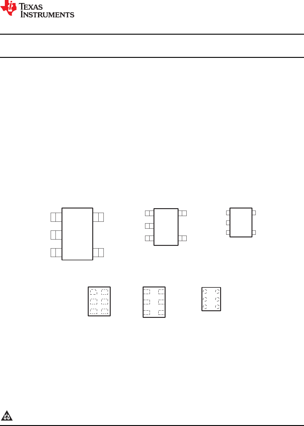
DNU – Do not use
N.C. – No internal connection
See mechanical drawings for dimensions.
DBV PACKAGE
(TOP VIEW)
5
1
2
V
CC
Y43
A
B
GND
DCK PACKAGE
(TOP VIEW)
5
1
2
V
CC
Y
4
3
A
B
GND
DRL PACKAGE
(TOP VIEW)
5
1
2
V
CC
Y
4
3
A
B
GND
DRY PACKAGE
(TOP VIEW)
B N.C.
A
6
5
4
2
3
GND
Y
V
CC
1
GND Y
3
4
B
2
5
A
6
1
N.C.
V
CC
DSF PACKAGE
(TOP VIEW)
YFP PACKAGE
( VIEW)TOP
GND
A
Y
V
CC
B
3
6
2
1
4
5
DNU
A1
B1
C1
A2
B2
C2
SN74AUP1G02
www.ti.com
SCES568G –JUNE 2004–REVISED MARCH 2010
LOW-POWER SINGLE 2-INPUT POSITIVE-NOR GATE
Check for Samples: SN74AUP1G02
1
FEATURES
• Available in the Texas Instruments NanoStar™ • Wide Operating V
CC
Range of 0.8 V to 3.6 V
Package
• Optimized for 3.3-V Operation
• Low Static-Power Consumption
• 3.6-V I/O Tolerant to Support Mixed-Mode
(I
CC
= 0.9 mA Max)
Signal Operation
• Low Dynamic-Power Consumption
• t
pd
= 4.6 ns Max at 3.3 V
(C
pd
= 4.3 pF Typ at 3.3 V)
• Suitable for Point-to-Point Applications
• Low Input Capacitance (C
i
= 1.5 pF Typ)
• Latch-Up Performance Exceeds 100 mA Per
• Low Noise – Overshoot and Undershoot
JESD 78, Class II
<10% of V
CC
• ESD Performance Tested Per JESD 22
• I
off
Supports Partial-Power-Down Mode
– 2000-V Human-Body Model
Operation
(A114-B, Class II)
• Input Hysteresis Allows Slow Input Transition
– 1000-V Charged-Device Model (C101)
and Better Switching-Noise Immunity at the
Input (V
hys
= 250 mV Typ at 3.3 V)
DESCRIPTION/ORDERING INFORMATION
The AUP family is TI's premier solution to the industry's low-power needs in battery-powered portable
applications. This family ensures a very low static- and dynamic-power consumption across the entire V
CC
range
of 0.8 V to 3.6 V, resulting in increased battery life (see Figure 1). This product also maintains excellent signal
integrity (see Figure 1 and Figure 2).
1
Please be aware that an important notice concerning availability, standard warranty, and use in critical applications of Texas
Instruments semiconductor products and disclaimers thereto appears at the end of this data sheet.
PRODUCTION DATA information is current as of publication date.
Copyright © 2004–2010, Texas Instruments Incorporated
Products conform to specifications per the terms of the Texas
Instruments standard warranty. Production processing does not
necessarily include testing of all parameters.