
Datasheet


Table Of Contents
- FEATURES
- DESCRIPTION/ORDERING INFORMATION
- ABSOLUTE MAXIMUM RATINGS
- RECOMMENDED OPERATING CONDITIONS
- ELECTRICAL CHARACTERISTICS
- SWITCHING CHARACTERISTICS
- SWITCHING CHARACTERISTICS
- SWITCHING CHARACTERISTICS
- SWITCHING CHARACTERISTICS
- OPERATING CHARACTERISTICS
- PARAMETER MEASUREMENT INFORMATION(Propagation Delays, Setup and Hold Times, and Pulse Width)
- PARAMETER MEASUREMENT INFORMATION(Enable and Disable Times)
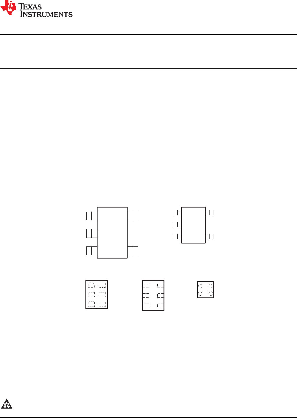
DBV PACKAGE
(TOP VIEW)
5
1
V
CC
N.C.
2
A
3
4
GND Y
DCK PACKAGE
(TOP VIEW)
2
A
3
4
GND
V
CC
5
N.C.
Y
1
YFP PACKAGE
(TOP VIEW)
A
V
CC
GND Y
DRY PACKAGE
(TOP VIEW)
A N.C.
N.C.
6
5
4
2
3
GND
Y
V
CC
1
GND Y
3
4
A
2
5
N.C.
6
1
N.C.
V
CC
DSF PACKAGE
(TOP VIEW)
4
2
1
A1
B1
A2
3
B2
SN74AUP1G06
www.ti.com
SCES590D –JULY 2004–REVISED MAY 2010
LOW-POWER SINGLE INVERTER BUFFER/DRIVER
WITH OPEN-DRAIN OUTPUTS
Check for Samples: SN74AUP1G06
1
FEATURES
2
• Available in the Texas Instruments NanoStar™
Input (V
hys
= 250 mV Typ at 3.3 V)
Package
• Wide Operating V
CC
Range of 0.8 V to 3.6 V
• Low Static-Power Consumption
• Optimized for 3.3-V Operation
(I
CC
= 0.9 μA Max)
• 3.6-V I/O Tolerant to Support Mixed-Mode
• Low Dynamic-Power Consumption
Signal Operation
(C
pd
= 1 pF Typ at 3.3 V)
• t
pd
= 3.6 ns Max at 3.3 V
• Low Input Capacitance (C
i
= 1.5 pF Typ)
• Suitable for Point-to-Point Applications
• Low Noise – Overshoot and Undershoot <10%
• Latch-Up Performance Exceeds 100 mA Per
of V
CC
JESD 78, Class II
• I
off
Supports Partial Power-Down-Mode
• ESD Performance Tested Per JESD 22
Operation
– 2000-V Human-Body Model
• Input Hysteresis Allows Slow Input Transition
(A114-B, Class II)
and Better Switching Noise Immunity at the
– 1000-V Charged-Device Model (C101)
See mechanical drawings for dimensions.
N.C. – No internal connection
1
Please be aware that an important notice concerning availability, standard warranty, and use in critical applications of
Texas Instruments semiconductor products and disclaimers thereto appears at the end of this data sheet.
2NanoStar is a trademark of Texas Instruments.
PRODUCTION DATA information is current as of publication date.
Copyright © 2004–2010, Texas Instruments Incorporated
Products conform to specifications per the terms of the Texas
Instruments standard warranty. Production processing does not
necessarily include testing of all parameters.