
Datasheet


SCES566F − MAY 2004 − REVISED APRIL 2005
1
POST OFFICE BOX 655303 • DALLAS, TEXAS 75265
D Control Inputs V
IH
/V
IL
Levels are
Referenced to V
CCA
Voltage
D V
CC
Isolation Feature − If Either V
CC
Input
Is at GND, Both Ports Are in the
High-Impedance State
D Overvoltage-Tolerant Inputs/Outputs Allow
Mixed-Voltage-Mode Data Communications
D Fully Configurable Dual-Rail Design Allows
Each Port to Operate Over the Full 1.2-V to
3.6-V Power-Supply Range
D I
off
Supports Partial-Power-Down Mode
Operation
D I/Os Are 4.6-V Tolerant
D Max Data Rates
− 380 Mbps (1.8-V to 3.3-V Translation)
− 260 Mbps (< 1.8-V to 3.3-V Translation)
− 260 Mbps (Translate to 2.5 V)
− 210 Mbps (Translate to 1.8 V)
− 120 Mbps (Translate to 1.5 V)
− 100 Mbps (Translate to 1.2 V)
D Latch-Up Performance Exceeds 100 mA Per
JESD 78, Class II
D ESD Protection Exceeds JESD 22
− 8000-V Human-Body Model (A114-A)
− 200-V Machine Model (A115-A)
− 1000-V Charged-Device Model (C101)
description/ordering information
This 20-bit noninverting bus transceiver uses two
separate configurable power-supply rails.
The SN74AVC20T245 is optimized to operate with V
CCA
/V
CCB
set at 1.4 V to 3.6 V. It is operational with
V
CCA
/V
CCB
as low as 1.2 V. The A port is designed to track V
CCA
. V
CCA
accepts any supply voltage from
1.2 V to 3.6 V. The B port is designed to track V
CCB
. V
CCB
accepts any supply voltage from 1.2 V to 3.6 V. This
allows for universal low-voltage bidirectional translation between any of the 1.2-V, 1.5-V, 1.8-V, 2.5-V, and 3.3-V
voltage nodes.
ORDERING INFORMATION
T
A
PACKAGE
†
ORDERABLE
PART NUMBER
TOP-SIDE
MARKING
TSSOP − DGG Tape and reel SN74AVC20T245DGGR AVC20T245
−40°C to 85°C
TVSOP − DGV Tape and reel SN74AVC20T245DGVR WG245
−40
°
C to 85
°
C
VFBGA − GQL
Tape and reel
SN74AVC20T245GQLR
WG245
VFBGA − ZQL (Pb-free)
Tape and reel
SN74AVC20T245ZQLR
WG245
†
Package drawings, standard packing quantities, thermal data, symbolization, and PCB design guidelines are available
at www.ti.com/sc/package.
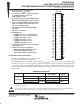
DGG OR DGV PACKAGE
(TOP VIEW)
1
2
3
4
5
6
7
8
9
10
11
12
13
14
15
16
17
18
19
20
21
22
23
24
25
26
27
28
56
55
54
53
52
51
50
49
48
47
46
45
44
43
42
41
40
39
38
37
36
35
34
33
32
31
30
29
1DIR
1B1
1B2
GND
1B3
1B4
V
CCB
1B5
1B6
1B7
GND
1B8
1B9
1B10
2B1
2B2
2B3
GND
2B4
2B5
2B6
V
CCB
2B7
2B8
GND
2B9
2B10
2DIR
1OE
1A1
1A2
GND
1A3
1A4
V
CCA
1A5
1A6
1A7
GND
1A8
1A9
1A10
2A1
2A2
2A3
GND
2A4
2A5
2A6
V
CCA
2A7
2A8
GND
2A9
2A10
2OE
Copyright 2005, Texas Instruments Incorporated
Please be aware that an important notice concerning availability, standard warranty, and use in critical applications of
Texas Instruments semiconductor products and disclaimers thereto appears at the end of this data sheet.
!"#$ % &'!!($ #% )'*+&#$ ,#$(-
!,'&$% &!" $ %)(&&#$% )(! $.( $(!"% (/#% %$!'"($%
%$#,#!, 0#!!#$1- !,'&$ )!&(%%2 ,(% $ (&(%%#!+1 &+',(
$(%$2 #++ )#!#"($(!%-