
Datasheet


SDFS040A − MARCH 1987 − REVISED OCTOBER 1993
Copyright 1993, Texas Instruments Incorporated
2−1
POST OFFICE BOX 655303 • DALLAS, TEXAS 75265
• Package Options Include Plastic
Small-Outline Packages, Ceramic Chip
Carriers, and Standard Plastic and Ceramic
300-mil DIPs
description
These devices contain three independent 3-input
AND gates. They perform the Boolean functions
Y = A • B • C or Y = A
+ B + C in positive logic.
The SN54F11 is characterized for operation over
the full military temperature range of −55°C to
125°C. The SN74F11 is characterized for
operation from 0°C to 70°C.
FUNCTION TABLE
(each gate)
INPUTS
OUTPUT
A B C
OUTPUT
Y
H H H H
L XX L
X LX L
X X L L
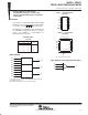
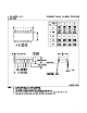
logic symbol
†
&
Y
1
1A
2
1B
13
1C
1Y
12
3
2A
4
2B
5
2C
2Y
6
9
3A
10
3B
11
3C
3Y
8
A
B
C
logic diagram, each gate (positive logic)
†
This symbol is in accordance with ANSI/IEEE Std 91-1984 and
IEC Publication 617-12.
Pin numbers shown are for the D, J, and N packages.
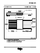
SN54F11 ...J PACKAGE
SN74F11 ...D OR N PACKAGE
(TOP VIEW)
SN54F11 . . . FK PACKAGE
(TOP VIEW)
3212019
910111213
4
5
6
7
8
18
17
16
15
14
1Y
NC
3C
NC
3B
2A
NC
2B
NC
2C
1B
1A
NC
3Y
3A
V
1C
2Y
GND
NC
CC
NC − No internal connection
1
2
3
4
5
6
7
14
13
12
11
10
9
8
1A
1B
2A
2B
2C
2Y
GND
V
CC
1C
1Y
3C
3B
3A
3Y
!" # $%&" !# '%()$!" *!"&+
*%$"# $ " #'&$$!"# '& ",& "&# &-!# #"%&"#
#"!*!* .!!"/+ *%$" '$&##0 *&# " &$&##!)/ $)%*&
"&#"0 !)) '!!&"&#+