
Datasheet


SN54F30, SN74F30
8-INPUT POSITIVE-NAND GATES
SDFS043A – MARCH 1987 – REVISED OCTOBER 1993
Copyright 1993, Texas Instruments Incorporated
2–1
POST OFFICE BOX 655303 • DALLAS, TEXAS 75265
• Package Options Include Plastic
Small-Outline Packages, Ceramic Chip
Carriers, and Standard Plastic and Ceramic
300-mil DIPs
description
These devices contain a single 8-input NAND
gate. They perform the Boolean functions
Y = A
• B • C • D • E • F • G • H or
Y = A
+ B + C + D + E + F + G + H in positive logic.
The SN54F30 is characterized for operation over
the full military temperature range of –55°C to
125°C. The SN74F30 is characterized for
operation from 0°C to 70°C.
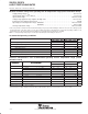
FUNCTION TABLE
INPUTS
A–H
OUTPUT
Y
All inputs H L
One or more inputs L H
logic symbol
†
&
Y
8
1
A
2
B
3
C
4
D
5
E
6
F
11
G
12
H
†
This symbol is in accordance with ANSI/IEEE Std 91-1984 and
IEC Publication 617-12.
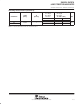
logic diagram (positive logic)
Y
8
1
A
2
B
3
C
4
D
5
E
6
F
11
G
12
H
Pin numbers shown are for the D, J, and N packages.
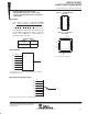
SN54F30 ...J PACKAGE
SN74F30 ...D OR N PACKAGE
(TOP VIEW)
SN54F30 . . . FK PACKAGE
(TOP VIEW)
3212019
910111213
4
5
6
7
8
18
17
16
15
14
H
NC
G
NC
NC
C
NC
D
NC
E
B
A
NC
Y
NC
V
NC
F
GND
NC
CC
NC – No internal connection
1
2
3
4
5
6
7
14
13
12
11
10
9
8
A
B
C
D
E
F
GND
V
CC
NC
H
G
NC
NC
Y
PRODUCTION DATA information is current as of publication date.
Products conform to specifications per the terms of Texas Instruments
standard warranty. Production processing does not necessarily include
testing of all parameters.