
Datasheet


SN74HC08-Q1
QUADRUPLE 2-INPUT POSITIVE-AND GATE
SCLS576C − MARCH 2004 − REVISED APRIL 2008
1
POST OFFICE BOX 655303 • DALLAS, TEXAS 75265
D Qualified for Automotive Applications
D Wide Operating Voltage Range of 2 V to 6 V
D Outputs Can Drive Up To 10 LSTTL Loads
D Low Power Consumption, 40-µA Max I
CC
D Typical t
pd
= 8 ns
D ±4-mA Output Drive at 5 V
D Low Input Current of 1 µA Max
description/ordering information
The SN74HC08 device contains four independent 2-input AND gates. They perform the Boolean function
Y + A • BorY+ A
) B
in positive logic.
ORDERING INFORMATION
{
T
A
PACKAGE
‡
ORDERABLE
PART NUMBER
TOP-SIDE
MARKING
−40°C to 85°C TSSOP − PW Tape and reel SN74HC08IPWRQ1 HC08I
40°C to 125°C
SOIC − D Tape and reel SN74HC08QDRQ1 HC08Q1
−40°C to 125°C
TSSOP − PW Tape and reel SN74HC08QPWRQ1 HC08Q1
†
For the most current package and ordering information, see the Package Option Addendum at the end of this
document, or see the TI web site at http://www.ti.com.
‡
Package drawings, thermal data, and symbolization are available at http://www.ti.com/packaging.
FUNCTION TABLE
(each gate)
INPUTS
OUTPUT
A B
OUTPUT
Y
H H H
L XL
X L L
logic diagram (positive logic)
A
B
Y
Please be aware that an important notice concerning availability, standard warranty, and use in critical applications of
Texas Instruments semiconductor products and disclaimers thereto appears at the end of this data sheet.
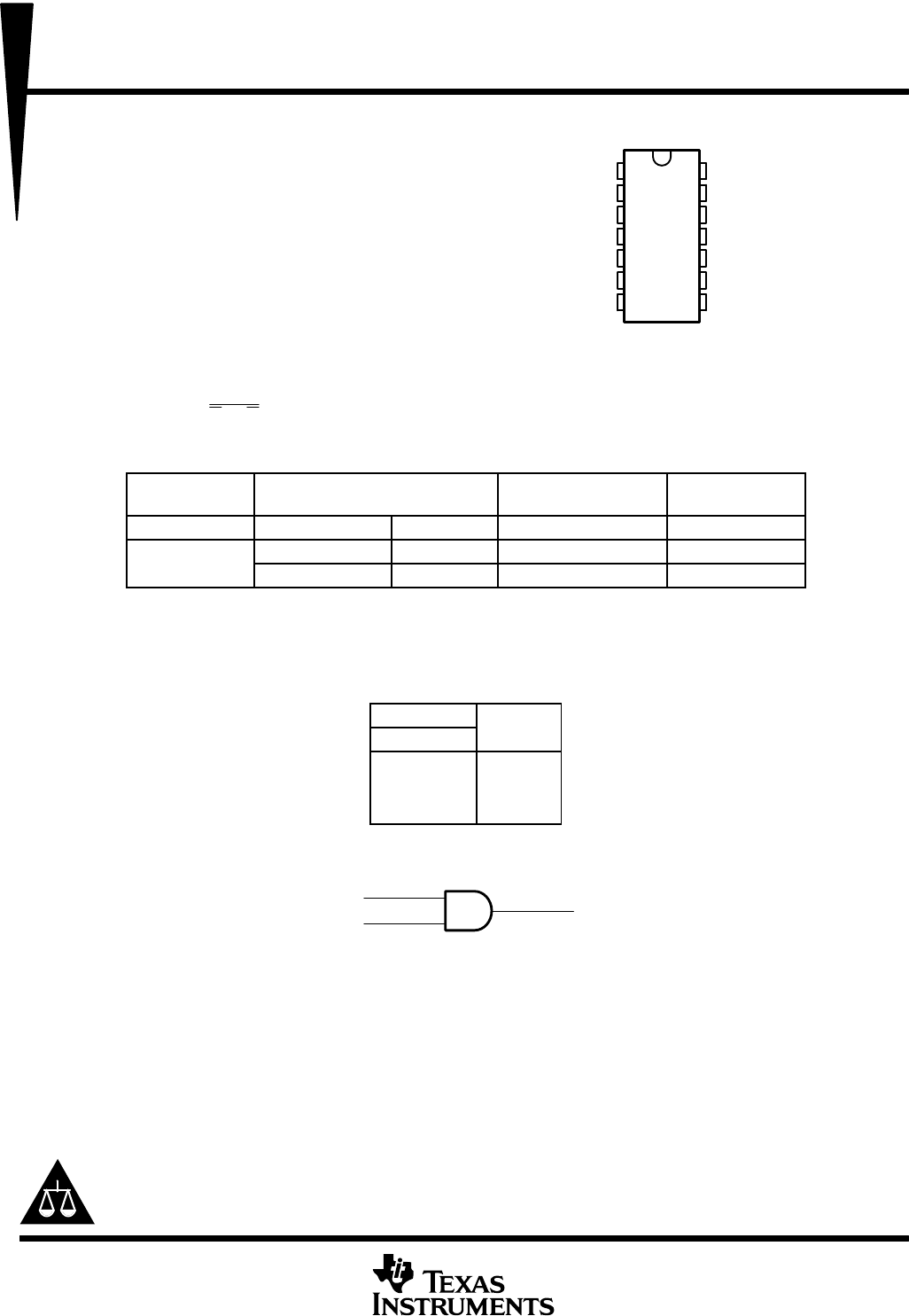
1
2
3
4
5
6
7
14
13
12
11
10
9
8
1A
1B
1Y
2A
2B
2Y
GND
V
CC
4B
4A
4Y
3B
3A
3Y
D OR PW PACKAGE
(TOP VIEW)
Copyright 2008, Texas Instruments Incorporated
PRODUCTION DATA information is current as of publication date.
Products conform to specifications per the terms of Texas Instruments
standard warranty. Production processing does not necessarily include
testing of all parameters.