
Datasheet


SCLS473A − APRIL 2003 − REVISED JANUARY 2004
1
POST OFFICE BOX 655303 • DALLAS, TEXAS 75265
D Controlled Baseline
− One Assembly/Test Site, One Fabrication
Site
D Extended Temperature Performance of Up
To −55°C to 125°C
D Enhanced Diminishing Manufacturing
Sources (DMS) Support
D Enhanced Product-Change Notification
D Qualification Pedigree
†
D 2-V to 6-V V
CC
Operation
D Outputs Can Drive Up To 10 LSTTL Loads
D Low Power Consumption, 80-µA Max I
CC
D Typical t
pd
= 13 ns
†
Component qualification in accordance with JEDEC and industry
standards to ensure reliable operation over an extended
temperature range. This includes, but is not limited to, Highly
Accelerated Stress Test (HAST) or biased 85/85, temperature
cycle, autoclave or unbiased HAST, electromigration, bond
intermetallic life, and mold compound life. Such qualification
testing should not be viewed as justifying use of this component
beyond specified performance and environmental limits.
D ±4-mA Output Drive at 5 V
D Low Input Current of 1 µA Max
D Complementary Outputs
D Direct Overriding Load (Data) Inputs
D Gated Clock Inputs
D Parallel-to-Serial Data Conversion
description/ordering information
The SN74HC165 is an 8-bit parallel-load shift register that, when clocked, shifts the data toward a serial (Q
H
)
output. Parallel-in access to each stage is provided by eight individual direct data (A−H) inputs that are enabled
by a low level at the shift/load (SH/LD
) input. The SN74HC165 device also features a clock-inhibit (CLK INH)
function and a complementary serial (Q
H
) output.
Clocking is accomplished by a low-to-high transition of the clock (CLK) input while SH/LD
is held high and CLK
INH is held low. The functions of CLK and CLK INH are interchangeable. Since a low CLK and a low-to-high
transition of CLK INH also accomplish clocking, CLK INH should be changed to the high level only while CLK
is high. Parallel loading is inhibited when SH/LD
is held high. While SH/LD is low, the parallel inputs to the
register are enabled independently of the levels of the CLK, CLK INH, or serial (SER) inputs.
ORDERING INFORMATION
T
A
PACKAGE
‡
ORDERABLE
PART NUMBER
TOP-SIDE
MARKING
−40°C to 125°C
SOIC − D Tape and reel SN74HC165QDREP HC165EP
−40°C to 125°C
TSSOP − PW Tape and reel SN74HC165QPWREP HC165EP
−55°C to 125°C SOIC − D Tape and reel SN74HC165MDREP HC165MEP
‡
Package drawings, standard packing quantities, thermal data, symbolization, and PCB design guidelines are
available at www.ti.com/sc/package.
Please be aware that an important notice concerning availability, standard warranty, and use in critical applications o
f
Texas Instruments semiconductor products and disclaimers thereto appears at the end of this data sheet.
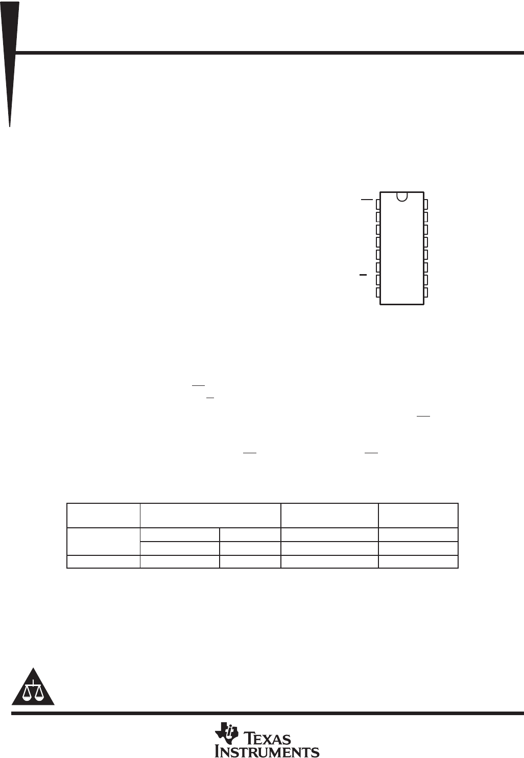
D OR PW PACKAGE
(TOP VIEW)
1
2
3
4
5
6
7
8
16
15
14
13
12
11
10
9
SH/LD
CLK
E
F
G
H
Q
H
GND
V
CC
CLK INH
D
C
B
A
SER
Q
H
Copyright 2004, Texas Instruments Incorporated
! " #$%! " &$'(#! )!%*
)$#!" # ! "&%##!" &% !+% !%" %," "!$%!"
"!)) -!.* )$#! &#%""/ )%" ! %#%""(. #($)%
!%"!/ (( &%!%"*