
Datasheet


SCLS310D − JANUARY 1996 −REVISED OCTOBER 2003
1
POST OFFICE BOX 655303 • DALLAS, TEXAS 75265
D Wide Operating Voltage Range of 2 V to 6 V
D High-Current 3-State Outputs Drive Bus
Lines, Buffer Memory Address Registers,
or Drive Up To 15 LSTTL Loads
D Inverting Outputs
D Low Power Consumption, 80-µA Max I
CC
D Typical t
pd
= 10 ns
D ±6-mA Output Drive at 5 V
D Low Input Current of 1 µA Max
description/ordering information
These hex inverting buffers and line drivers are
designed specifically to improve both the
performance and density of 3-state memory
address drivers, clock drivers, and bus-oriented
receivers and transmitters. The ’HC368 devices
are organized as dual 4-line and 2-line
buffers/drivers with active-low output-enable
(1OE
and 2OE) inputs. When OE is low, the
device passes inverted data from the A inputs to
the Y outputs. When OE
is high, the outputs are
in the high-impedance state.
ORDERING INFORMATION
T
A
PACKAGE
†
ORDERABLE
PART NUMBER
TOP-SIDE
MARKING
PDIP − N Tube of 25 SN74HC368N SN74HC368N
Tube of 40 SN74HC368D
SOIC − D
Reel of 2500 SN74HC368DR
HC368
SOIC − D
Reel of 250 SN74HC368DT
HC368
−40°C to 85°C
SOP − NS Reel of 2000 SN74HC368NSR HC368
−40 C to 85 C
SSOP − DB Reel of 2000 SN74HC368DBR HC368
Tube of 90 SN74HC368PW
TSSOP − PW
Reel of 2000 SN74HC368PWR
HC368
TSSOP − PW
Reel of 250 SN74HC368PWT
HC368
CDIP − J Tube of 25 SNJ54HC368J SNJ54HC368J
−55°C to 125°C
CFP − W Tube of 150 SNJ54HC368W SNJ54HC368W
−55 C to 125 C
LCCC − FK Tube of 55 SNJ54HC368FK SNJ54HC368FK
†
Package drawings, standard packing quantities, thermal data, symbolization, and PCB design guidelines are
available at www.ti.com/sc/package.
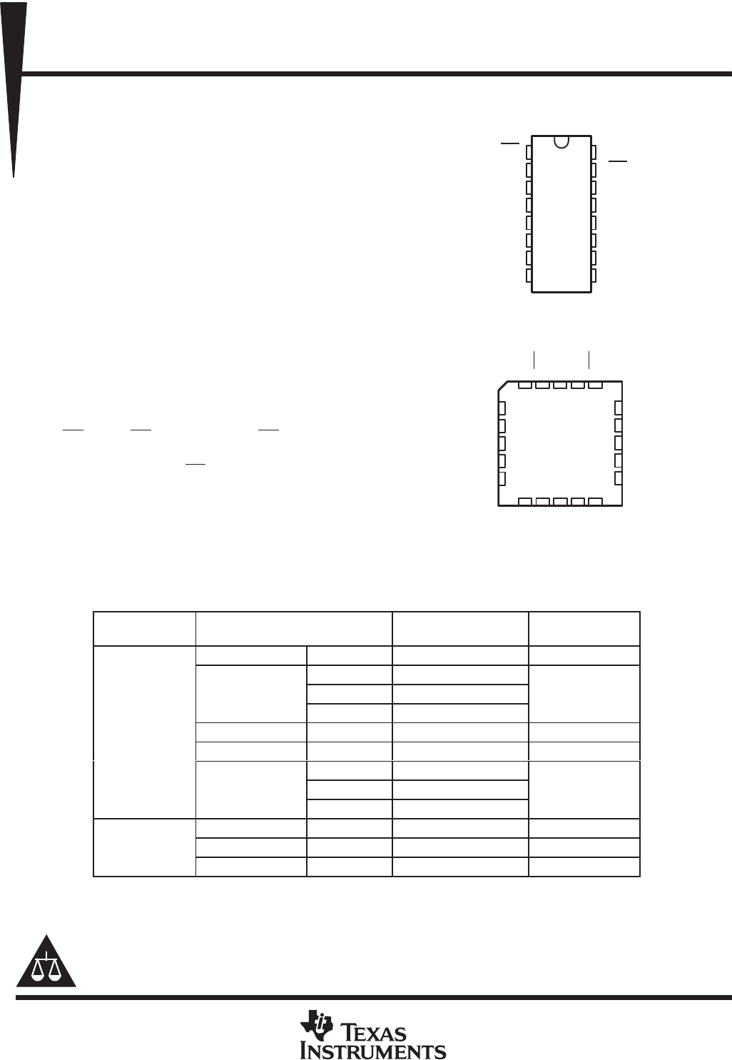
3212019
910111213
4
5
6
7
8
18
17
16
15
14
2A2
2Y2
NC
2A1
2Y1
1Y1
1A2
NC
1Y2
1A3
1A1
1OE
NC
1Y4
1A4
V
2OE
1Y3
GND
NC
SN54HC368 . . . FK PACKAGE
(TOP VIEW)
CC
NC − No internal connection
1
2
3
4
5
6
7
8
16
15
14
13
12
11
10
9
1OE
1A1
1Y1
1A2
1Y2
1A3
1Y3
GND
V
CC
2OE
2A2
2Y2
2A1
2Y1
1A4
1Y4
SN54HC368 ...J OR W PACKAGE
SN74HC368 . . . D, DB, N, NS, OR PW PACKAGE
(TOP VIEW)
Copyright 2003, Texas Instruments Incorporated
Please be aware that an important notice concerning availability, standard warranty, and use in critical applications of
Texas Instruments semiconductor products and disclaimers thereto appears at the end of this data sheet.
!"#$%! & '("")% $& ! *(+,'$%! -$%).
"!-('%& '!!"# %! &*)''$%!& *)" %/) %)"#& ! )0$& &%"(#)%&
&%$-$"- 1$""$%2. "!-('%! *"!')&&3 -!)& !% )')&&$",2 ',(-)
%)&%3 ! $,, *$"$#)%)"&.
*"!-('%& '!#*,$% %! 4 $,, *$"$#)%)"& $") %)&%)-
(,)&& !%/)"1&) !%)-. $,, !%/)" *"!-('%& *"!-('%!
*"!')&&3 -!)& !% )')&&$",2 ',(-) %)&%3 ! $,, *$"$#)%)"&.