
Datasheet
SN54HC563, SN74HC563
OCTAL TRANSPARENT D-TYPE LATCHES
WITH 3-STATE OUTPUTS
SCLS145C – DECEMBER 1982 – REVISED MARCH 2003
1
POST OFFICE BOX 655303 • DALLAS, TEXAS 75265
Wide Operating Voltage Range of 2 V to 6 V
High-Current 3-State Outputs Drive Bus
Lines Directly or Up To 15 LSTTL Loads
Low Power Consumption, 80-µA Max I
CC
Typical t
pd
= 21 ns
±6-mA Output Drive at 5 V
Low Input Current of 1 µA Max
Bus-Structured Pinout
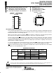
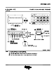
1
2
3
4
5
6
7
8
9
10
20
19
18
17
16
15
14
13
12
11
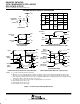
OE
1D
2D
3D
4D
5D
6D
7D
8D
GND
V
CC
1Q
2Q
3Q
4Q
5Q
6Q
7Q
8Q
LE
SN54HC563 ...J OR W PACKAGE
SN74HC563 . . . DW OR N PACKAGE
(TOP VIEW)
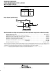
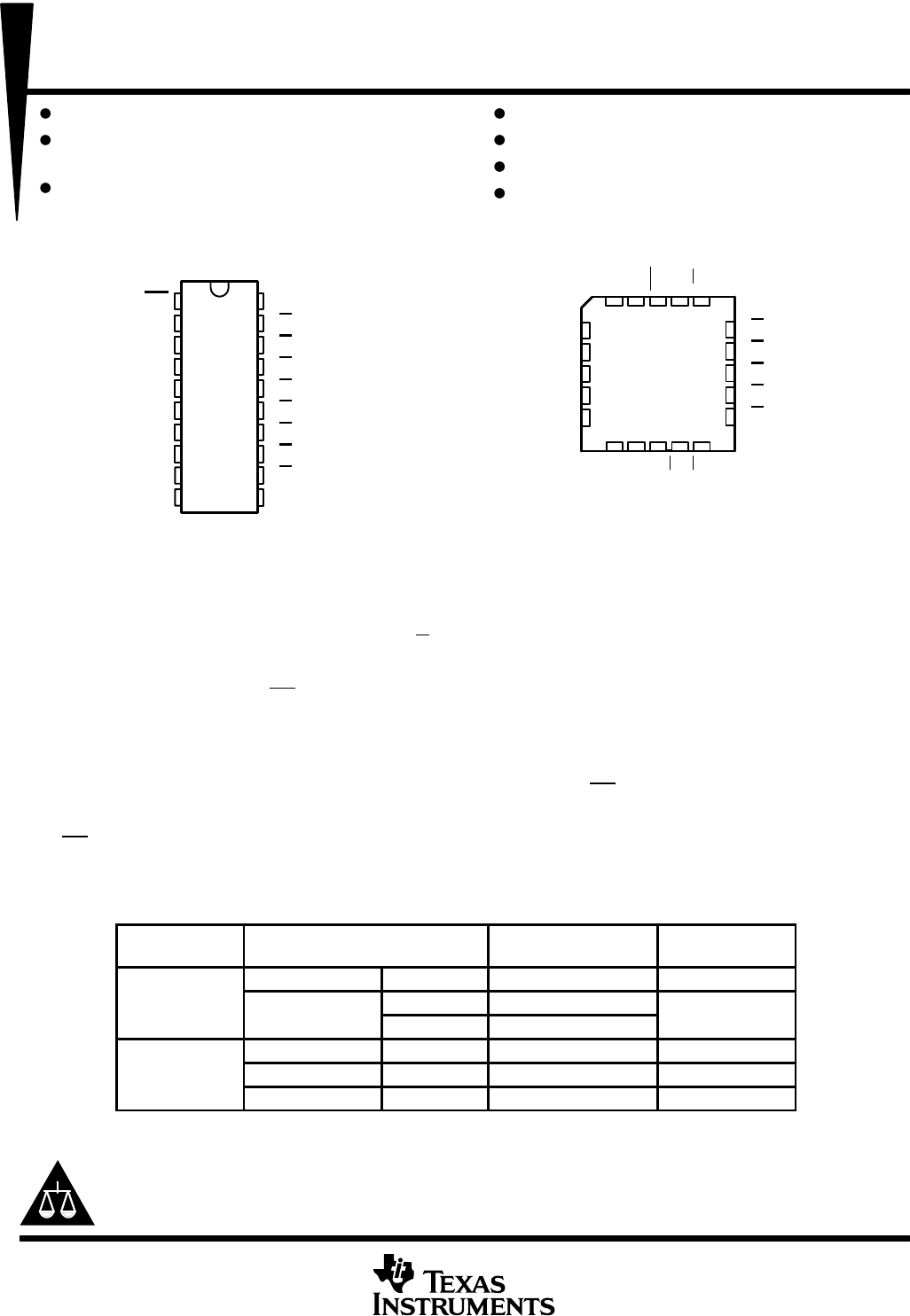
3212019
910111213
4
5
6
7
8
18
17
16
15
14
2Q
3Q
4Q
5Q
6Q
3D
4D
5D
6D
7D
SN54HC563 . . . FK PACKAGE
(TOP VIEW)
2D
1D
OE
8Q
7Q 1Q
8D
GND
LE
V
CC
description/ordering information
These 8-bit transparent D-type latches feature 3-state outputs designed specifically for driving highly capacitive
or relatively low-impedance loads. They are particularly suitable for implementing buffer registers, I/O ports,
bidirectional bus drivers, and working registers.
While the latch-enable (LE) input is high, the Q
outputs follow the complements of the data (D) inputs. When
LE is taken low, the outputs are latched at the inverses of the levels set up at the D inputs.
A buffered output-enable (OE
) input places the eight outputs in either a normal logic state (high or low logic
levels) or the high-impedance state. In the high-impedance state, the outputs neither load nor drive the bus lines
significantly. The high-impedance state and increased high logic level provide the capability to drive bus lines
without interface or pullup components.
To ensure the high-impedance state during power up or power down, OE
should be tied to V
CC
through a pullup
resistor; the minimum value of the resistor is determined by the current-sinking capability of the driver.
OE
does not affect internal operations of the latches. Old data can be retained or new data can be entered while
the outputs are in the high-impedance state.
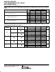
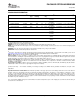
ORDERING INFORMATION
T
A
PACKAGE
†
ORDERABLE
PART NUMBER
TOP-SIDE
MARKING
PDIP – N Tube SN74HC563N SN74HC563N
–40°C to 85°C
SOIC DW
Tube SN74HC563DW
HC563
SOIC
–
DW
Tape and reel SN74HC563DWR
HC563
CDIP – J Tube SNJ54HC563J SNJ54HC563J
–55°C to 125°C
CFP – W Tube SNJ54HC563W SNJ54HC563W
LCCC – FK Tube SNJ54HC563FK SNJ54HC563FK
†
Package drawings, standard packing quantities, thermal data, symbolization, and PCB design guidelines are
available at www.ti.com/sc/package.
Copyright 2003, Texas Instruments Incorporated
Please be aware that an important notice concerning availability, standard warranty, and use in critical applications of
Texas Instruments semiconductor products and disclaimers thereto appears at the end of this data sheet.
UNLESS OTHERWISE NOTED this document contains PRODUCTION
DATA information current as of publication date. Products conform to
specifications per the terms of Texas Instruments standard warranty.
Production processing does not necessarily include testing of all
parameters.