
Datasheet

SN54HC563, SN74HC563
OCTAL TRANSPARENT D-TYPE LATCHES
WITH 3-STATE OUTPUTS
SCLS145C – DECEMBER 1982 – REVISED MARCH 2003
3
POST OFFICE BOX 655303 • DALLAS, TEXAS 75265
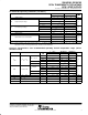
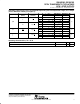
recommended operating conditions (see Note 3)
SN54HC563 SN74HC563
UNIT
MIN NOM MAX MIN NOM MAX
UNIT
V
CC
Supply voltage 2 5 6 2 5 6 V
V
CC
= 2 V 1.5 1.5
V
IH
High-level input voltage
V
CC
= 4.5 V
3.15 3.15
V
V
CC
= 6 V 4.2 4.2
V
CC
= 2 V 0.5 0.5
V
IL
Low-level input voltage
V
CC
= 4.5 V
1.35 1.35
V
V
CC
= 6 V 1.8 1.8
V
I
Input voltage 0 V
CC
0 V
CC
V
V
O
Output voltage 0 V
CC
0 V
CC
V
V
CC
= 2 V 1000 1000
t
t
Input transition (rise and fall) time
V
CC
= 4.5 V
500 500
ns
V
CC
= 6 V 400 400
T
A
Operating free-air temperature –55 125 –40 85 °C
NOTE 3: All unused inputs of the device must be held at V
CC
or GND to ensure proper device operation. Refer to the TI application report,
Implications of Slow or Floating CMOS Inputs, literature number SCBA004.
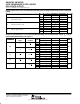
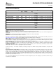
electrical characteristics over recommended operating free-air temperature range (unless
otherwise noted)
PARAMETER
TEST CONDITIONS
V
CC
T
A
= 25°C SN54HC563 SN74HC563
UNIT
PARAMETER
TEST
CONDITIONS
V
CC
MIN TYP MAX MIN MAX MIN MAX
UNIT
2 V 1.9 1.998 1.9 1.9
I
OH
= –20 µA
4.5 V 4.4 4.499 4.4 4.4
V
OH
V
I
= V
IH
or V
IL
6 V 5.9 5.999 5.9 5.9
V
I
OH
= –6 mA 4.5 V 3.98 4.3 3.7 3.84
I
OH
= –7.8 mA 6 V 5.48 5.8 5.2 5.34
2 V 0.002 0.1 0.1 0.1
I
OL
= 20 µA
4.5 V 0.001 0.1 0.1 0.1
V
OL
V
I
= V
IH
or V
IL
6 V 0.001 0.1 0.1 0.1
V
I
OL
= 6 mA 4.5 V 0.17 0.26 0.4 0.33
I
OL
= 7.8 mA 6 V 0.15 0.26 0.4 0.33
I
I
V
I
= V
CC
or 0 6 V ±0.1 ±100 ±1000 ±1000 nA
I
OZ
V
O
= V
CC
or 0 6 V ±0.01 ±0.5 ±10 ±5 µA
I
CC
V
I
= V
CC
or 0, I
O
= 0 6 V 8 160 80 µA
C
i
2 V to 6 V 3 10 10 10 pF
PRODUCT PREVIEW information concerns products in the formative or
design phase of development. Characteristic data and other
specifications are design goals. Texas Instruments reserves the right to
change or discontinue these products without notice.