
Datasheet


www.ti.com
FEATURES
1
2
3
4
5
6
7
14
13
12
11
10
9
8
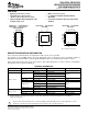
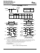
1A
1Y
2A
2Y
3A
3Y
GND
V
CC
6A
6Y
5A
5Y
4A
4Y
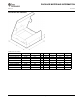
SN54LVC06A . . . J OR W PACKAGE
SN74LVC06A . . . D, DB, DGV, NS,
OR PW PACKAGE
(TOP VIEW)
3 2 1 20 19
9 10 11 12 13
4
5
6
7
8
18
17
16
15
14
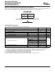
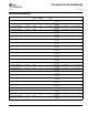
6Y
NC
5A
NC
5Y
2A
NC
2Y
NC
3A
SN54LVC06A . . . FK PACKAGE
(TOP VIEW)
1Y
1A
NC
4Y
4A
6A
3Y
GND
NC
V
CC
NC - No internal connection
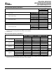
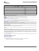
SN74LVC06A . . . RGY PACKAGE
(TOP VIEW)
1 14
7 8
2
3
4
5
6
13
12
11
10
9
6A
6Y
5A
5Y
4A
1Y
2A
2Y
3A
3Y
1A
4Y
V
GND
CC
DESCRIPTION/ORDERING INFORMATION
SN54LVC06A, SN74LVC06A
HEX INVERTER BUFFERS/DRIVERS
WITH OPEN-DRAIN OUTPUTS
SCAS596N – OCTOBER 1997 – REVISED JULY 2005
• Operate From 1.65 V to 3.6 V • Max t
pd
of 3.7 ns at 3.3 V
• Specified From –40 ° C to 85 ° C, • I
off
Supports Partial-Power-Down Mode
–40 ° C to 125 ° C, and –55 ° C to 125 ° C Operation
• Inputs and Open-Drain Outputs Accept • Latch-Up Performance Exceeds 250 mA Per
Voltages up to 5.5 V JESD 17
These hex inverter buffers/drivers are designed for 1.65-V to 3.6-V V
CC
operation.
The outputs of the 'LVC06A devices are open drain and can be connected to other open-drain outputs to
implement active-low wired-OR or active-high wired-AND functions. The maximum sink current is 24 mA.
Inputs can be driven from either 3.3-V or 5-V devices. This feature allows the use of these devices as translators
in a mixed 3.3-V/5-V system environment.
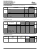
ORDERING INFORMATION
T
A
PACKAGE
(1)
ORDERABLE PART NUMBER TOP-SIDE MARKING
–40 ° C to 85 ° C QFN – RGY Reel of 1000 SN74LVC06ARGYR LC06A
Tube of 50 SN74LVC06AD
SOIC – D Reel of 2500 SN74LVC06ADR LVC06A
Reel of 250 SN74LVC06ADT
SOP – NS Reel of 2000 SN74LVC06ANSR LVC06A
–40 ° C to 125 ° C SSOP – DB Reel of 2000 SN74LVC06ADBR LC06A
Tube of 90 SN74LVC06APW
TSSOP – PW Reel of 2000 SN74LVC06APWR LC06A
Reel of 250 SN74LVC06APWT
TVSOP – DGV Reel of 2000 SN74LVC06ADGVR LC06A
CDIP – J Tube of 25 SNJ54LVC06AJ SNJ54LVC06AJ
–55 ° C to 125 ° C CFP – W Tube of 150 SNJ54LVC06AW SNJ54LVC06AW
LCCC – FK Tube of 55 SNJ54LVC06AFK SNJ54LVC06AFK
(1) Package drawings, standard packing quantities, thermal data, symbolization, and PCB design guidelines are available at
www.ti.com/sc/package.
Please be aware that an important notice concerning availability, standard warranty, and use in critical applications of Texas
Instruments semiconductor products and disclaimers thereto appears at the end of this data sheet.
UNLESS OTHERWISE NOTED this document contains PRO-
Copyright © 1997–2005, Texas Instruments Incorporated
DUCTION DATA information current as of publication date. Prod-
ucts conform to specifications per the terms of Texas Instruments
standard warranty. Production processing does not necessarily
include testing of all parameters.