
Datasheet
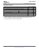


Absolute Maximum Ratings
(1)
SN74LVC1G04-EP
www.ti.com
................................................................................................................................................. SCES691A – MARCH 2007 – REVISED OCTOBER 2008
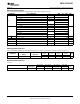
over operating free-air temperature range (unless otherwise noted)
MIN MAX UNIT
V
CC
Supply voltage range – 0.5 6.5 V
V
I
Input voltage range – 0.5 6.5 V
V
O
Voltage range applied to any output in the high-impedance or power-off state
(2)
– 0.5 6.5 V
V
O
Voltage range applied to any output in the high or low state
(2) (3)
– 0.5 V
CC
+ 0.5 V
I
IK
Input clamp current V
I
< 0 – 50 mA
I
OK
Output clamp current V
O
< 0 – 50 mA
I
O
Continuous output current ± 50 mA
Continuous current through V
CC
or GND ± 100 mA
θ
JA
Package thermal impedance
(4)
206 ° C/W
T
stg
Storage temperature range – 65 150 ° C
(1) Stresses beyond those listed under " absolute maximum ratings " may cause permanent damage to the device. These are stress ratings
only, and functional operation of the device at these or any other conditions beyond those indicated under " recommended operating
conditions " is not implied. Exposure to absolute-maximum-rated conditions for extended periods may affect device reliability.
(2) The input and output negative-voltage ratings may be exceeded if the input and output current ratings are observed.
(3) The value of V
CC
is provided in the recommended operating conditions table.
(4) The package thermal impedance is calculated in accordance with JESD 51-7.
Copyright © 2007 – 2008, Texas Instruments Incorporated Submit Documentation Feedback 3
Product Folder Link(s): SN74LVC1G04-EP