
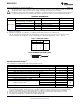
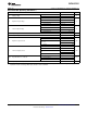
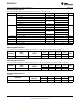
Datasheet

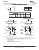


See mechanical drawings for dimensions.
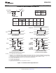
DBV PACKAGE
(TOP VIEW)
2
GND
V
CC
5
3
4
B
Y
6
1
A
C
DCK PACKAGE
(TOP VIEW)
3
4
B
2
GND
Y
5
1
A
V
CC
6
C
DRY PACKAGE
(TOP VIEW)
GND
V
CC
A
6
5
4
2
3
B Y
C
1
YZP PACKAGE
(BOTTOM VIEW)
GND V
CC
A
B
2
1
3
Y
5
4
6
C
A
B
DSF PACKAGE
(TOP VIEW)
GND
C
Y
V
CC
6
5
4
2
3
1
Y + A • B • C or Y + A ) B ) C
SN74LVC1G11
www.ti.com
SCES487E –SEPTEMBER 2003–REVISED DECEMBER 2011
SINGLE 3-INPUT POSITIVE-AND GATE
Check for Samples: SN74LVC1G11
1
FEATURES
2
• Available in the Texas Instruments NanoFree™
• Latch-Up Performance Exceeds 100 mA Per
Package JESD 78, Class II
• Supports 5-V V
CC
Operation • ESD Protection Exceeds JESD 22
• Inputs Accept Voltages to 5.5 V – 2000-V Human-Body Model (A114-A)
• Max t
pd
of 4.1 ns at 3.3 V – 200-V Machine Model (A115-A)
• Low Power Consumption, 10-μA Max I
CC
– 1000-V Charged-Device Model (C101)
• ±24-mA Output Drive at 3.3 V
• I
off
Supports Partial-Power-Down Mode
Operation
DESCRIPTION/ORDERING INFORMATION
The SN74LVC1G11 performs the Boolean function in positive logic.
NanoFree™ package technology is a major breakthrough in IC packaging concepts, using the die as the
package.
This device is fully specified for partial-power-down applications using I
off
. The I
off
circuitry disables the outputs,
preventing damaging current backflow through the device when it is powered down.
1
Please be aware that an important notice concerning availability, standard warranty, and use in critical applications of
Texas Instruments semiconductor products and disclaimers thereto appears at the end of this data sheet.
2NanoFree is a trademark of Texas Instruments.
PRODUCTION DATA information is current as of publication date.
Copyright © 2003–2011, Texas Instruments Incorporated
Products conform to specifications per the terms of the Texas
Instruments standard warranty. Production processing does not
necessarily include testing of all parameters.