
Datasheet

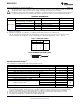


A
C
Y
B
SN74LVC1G11
SCES487E –SEPTEMBER 2003–REVISED DECEMBER 2011
www.ti.com
This integrated circuit can be damaged by ESD. Texas Instruments recommends that all integrated circuits be handled with
appropriate precautions. Failure to observe proper handling and installation procedures can cause damage.
ESD damage can range from subtle performance degradation to complete device failure. Precision integrated circuits may be more
susceptible to damage because very small parametric changes could cause the device not to meet its published specifications.
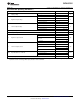
ORDERING INFORMATION
T
A
PACKAGE
(1)
ORDERABLE PART NUMBER TOP-SIDE MARKING
(2)
NanoFree™ – WCSP (DSBGA)
Reel of 3000 SN74LVC1G11YZPR _ _ _C3_
0.23-mm Large Bump – YZP (Pb-free)
SOT (SOT-23) – DBV Reel of 3000 SN74LVC1G11DBVR C11_
–40°C to 85°C
QFN – DRY Reel of 5000 SN74LVC1G11DRYR C3
µQFN – DSF Reel of 5000 SN74LVC1G11DSFR C3
SOT (SC-70) – DCK Reel of 3000 SN74LVC1G11DCKR C3_
(1) Package drawings, standard packing quantities, thermal data, symbolization, and PCB design guidelines are available at
www.ti.com/sc/package.
(2) DBV/DCK: The actual top-side marking has one additional character that designates the assembly/test site.
YZP: The actual top-side marking has three preceding characters to denote year, month, and sequence code, and one following
character to designate the assembly/test site. Pin 1 identifier indicates solder-bump composition (1 = SnPb, • = Pb-free).
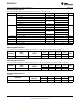
Table 1. FUNCTION TABLE
INPUTS
OUTPUT
Y
A B C
H H H H
L X X L
X L X L
X X L L
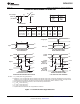
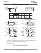
LOGIC DIAGRAM (POSITIVE LOGIC)
Absolute Maximum Ratings
(1)
over operating free-air temperature range (unless otherwise noted)
MIN MAX UNIT
V
CC
Supply voltage range –0.5 6.5 V
V
I
Input voltage range
(2)
–0.5 6.5 V
V
O
Voltage range applied to any output in the high-impedance or power-off state
(2)
–0.5 6.5 V
V
O
Voltage range applied to any output in the high or low state
(2) (3)
–0.5 V
CC
+ 0.5 V
I
IK
Input clamp current V
I
< 0 –50 mA
I
OK
Output clamp current V
O
< 0 –50 mA
I
O
Continuous output current ±50 mA
Continuous current through V
CC
or GND ±100 mA
DBV package 165
θ
JA
Package thermal impedance
(4)
DCK package 259 °C/W
YZP package 123
T
stg
Storage temperature range –65 150 °C
(1) Stresses beyond those listed under "absolute maximum ratings" may cause permanent damage to the device. These are stress ratings
only, and functional operation of the device at these or any other conditions beyond those indicated under "recommended operating
conditions" is not implied. Exposure to absolute-maximum-rated conditions for extended periods may affect device reliability.
(2) The input negative-voltage and output voltage ratings may be exceeded if the input and output current ratings are observed.
(3) The value of V
CC
is provided in the recommended operating conditions table.
(4) The package thermal impedance is calculated in accordance with JESD 51-7.
2 Submit Documentation Feedback Copyright © 2003–2011, Texas Instruments Incorporated
Product Folder Link(s): SN74LVC1G11