
Datasheet


t
h
t
su
FromOutput
UnderTest
C
(seeNote A)
L
LOADCIRCUIT
S1
V
LOAD
Open
GND
R
L
DataInput
TimingInput
0V
0V
0V
t
W
Input
0V
Input
Output
Waveform1
S1atV
(seeNoteB)
LOAD
Output
Waveform2
S1atGND
(seeNoteB)
V
OL
V
OH
0V
»0V
Output
Output
t /t
PLH PHL
Open
TEST S1
Output
Control
V
M
V
M
V
M
V
M
V
M
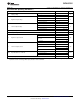
1.8V 0.15V±
2.5V 0.2V±
3.3V 0.3V±
5V 0.5V±
1MW
1MW
1MW
1MW
V
CC
R
L
2× V
CC
2× V
CC
6V
2× V
CC
V
LOAD
C
L
15pF
15pF
15pF
15pF
0.15V
0.15V
0.3V
0.3V
V
D
3V
V
I
V
CC
/2
V
CC
/2
1.5V
V
CC
/2
V
M
£2ns
£2ns
£2.5ns
£2.5ns
INPUTS
R
L
t /t
r f
V
CC
V
CC
V
CC
V
LOAD
t /t
PLZ PZL
GND
t /t
PHZ PZH
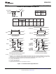
VOLTAGEWAVEFORMS
ENABLE ANDDISABLETIMES
LOW- ANDHIGH-LEVEL ENABLING
VOLTAGEWAVEFORMS
PROPAGATIONDELAY TIMES
INVERTING ANDNONINVERTINGOUTPUTS
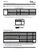
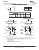
NOTES: A. C includesprobeandjigcapacitance.
B. Waveform1isforanoutputwithinternalconditionssuchthattheoutputislow,exceptwhendisabledbytheoutputcontrol.
Waveform2isforanoutputwithinternalconditionssuchthattheoutputishigh,exceptwhendisabledbytheoutputcontrol.
C. Allinputpulsesaresuppliedbygeneratorshavingthefollowingcharacteristics:PRR 10MHz,Z =50 .
D. Theoutputsaremeasuredoneatatime,withonetransitionpermeasurement.
E. t andt arethesameast .
F. t andt arethesameast .
G. t andt arethesameast .
H. Allparametersandwaveformsarenotapplicabletoalldevices.
L
O
PLZ PHZ dis
PZL PZH en
PLH PHL pd
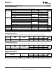
£ W
VOLTAGEWAVEFORMS
PULSEDURATION
VOLTAGEWAVEFORMS
SETUP ANDHOLDTIMES
V
I
V
I
V
I
V
M
V
M
V /2
LOAD
t
PZL
t
PLZ
t
PHZ
t
PZH
V – V
OH D
V +V
OL D
V
M
V
M
V
M
V
M
V
OL
V
OH
V
I
V
I
V
OH
V
OL
V
M
V
M
V
M
V
M
t
PLH
t
PHL
t
PLH
t
PHL
SN74LVC1G11
www.ti.com
SCES487E –SEPTEMBER 2003–REVISED DECEMBER 2011
PARAMETER MEASUREMENT INFORMATION
Figure 1. Load Circuit and Voltage Waveforms
Copyright © 2003–2011, Texas Instruments Incorporated Submit Documentation Feedback 5
Product Folder Link(s): SN74LVC1G11