
Datasheet


Table Of Contents
www.ti.com
FEATURES
Seemechanicaldrawingsfordimensions.
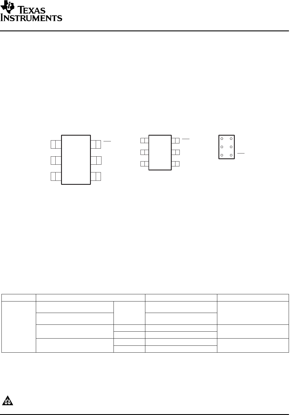
DBVPACKAGE
(TOP VIEW)
3
4
D
2
GND
Q
OE
V
CC
6
5
1
CLK
DCKPACKAGE
(TOP VIEW)
OE
3
4
D
2
GND
Q
6
5
1
CLK
V
CC
YEP OR YZP PACKAGE
(BOTTOMVIEW)
OE
2
GND
V
CC
1
6
CLK
D
4
5
3
Q
DESCRIPTION/ORDERING INFORMATION
SN74LVC1G374
SINGLE D-TYPE FLIP-FLOP WITH 3-STATE OUTPUT
SCES520B – DECEMBER 2003 – REVISED SEPTEMBER 2006
• Available in the Texas Instruments • Latch-Up Performance Exceeds 100 mA Per
NanoStar™ and NanoFree™ Packages JESD 78, Class II
• Supports 5-V V
CC
Operation • ESD Protection Exceeds JESD 22
• Inputs Accept Voltages to 5.5 V – 2000-V Human-Body Model (A114-A)
• Max t
pd
of 4 ns at 3.3 V – 200-V Machine Model (A115-A)
• Low Power Consumption, 10- µ A Max I
CC
– 1000-V Charged-Device Model (C101)
• ± 24-mA Output Drive at 3.3 V
• I
off
Supports Partial-Power-Down Mode
Operation
This single D-type latch is designed for 1.65-V to 5.5-V V
CC
operation.
The SN74LVC1G374 features a 3-state output designed specifically for driving highly capacitive or relatively
low-impedance loads. This device is particularly suitable for implementing buffer registers, input/output (I/O)
ports, bidirectional bus drivers, and working registers.
NanoStar™ and NanoFree™ package technology is a major breakthrough in IC packaging concepts, using the
die as the package.
On the positive transition of the clock (CLK) input, the Q output is set to the logic level set up at the data (D)
input.
ORDERING INFORMATION
T
A
PACKAGE
(1)
ORDERING PART NUMBER TOP-SIDE MARKING
(2)
NanoStar – WCSP (DSBGA)
SN74LVC1G374YEPR
0.23-mm Large Bump – YEP
Reel of 3000 _ _ _D4_
NanoFree – WCSP (DSBGA)
SN74LVC1G374YZPR
0.23-mm Large Bump – YZP (Pb-free)
–40 ° C to 85 ° C
Reel of 3000 SN74LVC1G374DBVR
SOT (SOT-23) – DBV CA4_ _ _
Reel of 250 SN74LVC1G374DBVT
Reel of 3000 SN74LVC1G374DCKR
SOT (SC-70) – DCK D4_
Reel of 250 SN74LVC1G374DCKT
(1) Package drawings, standard packing quantities, thermal data, symbolization, and PCB design guidelines are available at
www.ti.com/sc/package.
(2) DBV/DCK: The actual top-side marking has one additional character that designates the assembly/test site.
YEP/YZP: The actual top-side marking has three preceding characters to denote year, month, and sequence code, and one following
character to designate the assembly/test site. Pin 1 identifier indicates solder-bump composition(1 = SnPb, • = Pb-free).
Please be aware that an important notice concerning availability, standard warranty, and use in critical applications of Texas
Instruments semiconductor products and disclaimers thereto appears at the end of this data sheet.
NanoStar, NanoFree are trademarks of Texas Instruments.
PRODUCTION DATA information is current as of publication date.
Copyright © 2003–2006, Texas Instruments Incorporated
Products conform to specifications per the terms of the Texas
Instruments standard warranty. Production processing does not
necessarily include testing of all parameters.