
Datasheet


Seemechanicaldrawingsfordimensions.
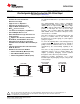
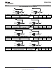
DCTPACKAGE
(TOP VIEW)
DCUPACKAGE
(TOP VIEW)
YZP PACKAGE
(BOTTOMVIEW)
1
V
CC
8
OE
2
7
A Y
3 6
B
D
4
5
GND
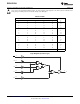
C
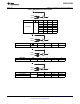
3 6
DB
8
1
V
CC
OE
5
GND
4
C
2
7
YA
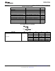
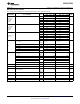
GND
5
4
C
3
6
DB
2
7
YA
8
V
CC
1
OE
SN74LVC1G99
www.ti.com
SCES609G –SEPTEMBER 2004–REVISED NOVEMBER 2013
Ultra-Configurable Multiple-Function Gate With 3-State Output
Check for Samples: SN74LVC1G99
1
FEATURES
DESCRIPTION
The SN74LVC1G99 device is operational from 1.65 V
2
• Available in Texas Instruments
to 5.5 V.
NanoFree™ Package
The SN74LVC1G99 device features configurable
• Supports 5-V V
CC
Operation
multiple functions with a 3-state output. The output is
• Inputs Accept Voltages to 5.5 V
disabled when the output-enable (OE) input is high.
• Supports Down Translation to V
CC
When OE is low, the output state is determined by 16
patterns of 4-bit input. The user can choose logic
• Max t
pd
of 6.7 ns at 3.3 V
functions, such as MUX, AND, OR, NAND, NOR,
• Low Power Consumption, 10-µA Max I
CC
XOR, XNOR, inverter, and buffer. All inputs can be
• ±24-mA Output Drive at 3.3 V
connected to V
CC
or GND.
• Offers Nine Different Logic Functions in a
This device functions as an independent inverter, but
Single Package
because of Schmitt action, it has different input
• I
off
Supports Live Insertion, Partial-Power-
threshold levels for positive-going (V
T+
) and negative-
Down Mode, and Back-Drive Protection
going (V
T–
) signals.
• Input Hysteresis Allows for Slow Input
To ensure the high-impedance state during power up
Transition Time and Better Noise Immunity at
or power down, OE should be tied to V
CC
through a
Input
pullup resistor; the minimum value of the resistor is
determined by the current-sinking capability of the
• Latch-Up Performance Exceeds 100 mA Per
driver.
JESD 78, Class II
This device is fully specified for partial-power-down
• ESD Protection Exceeds JESD 22
applications using I
off
. The I
off
circuitry disables the
– 2000-V Human-Body Model (A114-A)
outputs, preventing damaging current backflow
– 200-V Machine Model (A115-A)
through the device when it is powered down.
– 1000-V Charged-Device Model (C101)
NanoFree™ package technologies are a major
breakthrough in IC packaging concepts, using the die
as the package.
1
Please be aware that an important notice concerning availability, standard warranty, and use in critical applications of
Texas Instruments semiconductor products and disclaimers thereto appears at the end of this data sheet.
2NanoFree is a trademark of Texas Instruments.
PRODUCTION DATA information is current as of publication date.
Copyright © 2004–2013, Texas Instruments Incorporated
Products conform to specifications per the terms of the Texas
Instruments standard warranty. Production processing does not
necessarily include testing of all parameters.