
Datasheet


www.ti.com
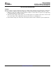
FEATURES
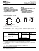
See mechanical drawings for dimensions.
DNU – Do not use
NC – No internal connection
DBV PACKAGE
(TOP VIEW)
6
5
1
Y
V
CC
NC
2
GND
3
4
X1 X2
DRL PACKAGE
(TOP VIEW)
2
GND
Y
V
CC
6
5
1
NC
3
4
X1
X2
DCK PACKAGE
(TOP VIEW)
2
GND
3
4
X1
Y
V
CC
6
5
NC
X2
1
YEP OR YZP PACKAGE
(BOTTOM VIEW)
2
GND
Y
V
CC
1
5
5
DNU
X1
4
3
X2
PREVIEW
DESCRIPTION/ORDERING INFORMATION
SN74LVC1GX04
CRYSTAL OSCILLATOR DRIVER
SCES581B – JULY 2004 – REVISED DECEMBER 2006
• Available in Texas Instruments NanoStar™ • ± 24-mA Output Drive at 3.3 V
and NanoFree™ Packages
• I
off
Supports Partial-Power-Down Mode
• Supports 5-V V
CC
Operation Operation
• Inputs Accept Voltages to 5.5 V • Latch-Up Performance Exceeds 100 mA Per
JESD 78, Class II
• One Unbuffered Inverter (SN74LVC1GU04)
and One Buffered Inverter (SN74LVC1G04) • ESD Protection Exceeds JESD 22
• Suitable for Commonly Used Clock – 2000-V Human-Body Model (A114-A)
Frequencies:
– 200-V Machine Model (A115-A)
– 15 kHz, 3.58 MHz, 4.43 MHz, 13 MHz,
– 1000-V Charged-Device Model (C101)
25 MHz, 26 MHz, 27 MHz, 28 MHz
• Max t
pd
of 2.4 ns at 3.3 V
• Low Power Consumption, 10- µ A Max I
CC
The SN74LVC1GX04 is designed for 1.65-V to 5.5-V V
CC
operation. This device incorporates the
SN74LVC1GU04 (inverter with unbuffered output) and the SN74LVC1G04 (inverter) functions into a single
device. The LVC1GX04 is optimized for use in crystal oscillator applications.
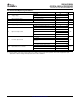
ORDERING INFORMATION
T
A
PACKAGE
(1)
ORDERABLE PART NUMBER TOP-SIDE MARKING
(2)
NanoStar™ – WCSP (DSBGA)
SN74LVC1GX04YEPR
(3)
PREVIEW
0.23-mm Large Bump – YEP
Reel of 3000
NanoFree™ – WCSP (DSBGA)
SN74LVC1GX04YZPR
(3)
PREVIEW
0.23-mm Large Bump – YZP (Pb-free)
Reel of 3000 SN74LVC1GX04DBVR
–40 ° C to 85 ° C
SOT (SOT-23) – DBV CX4_
Reel of 250 SN74LVC1GX04DBVT
Reel of 3000 SN74LVC1GX04DCKR
SOT (SC-70) – DCK D2_
Reel of 250 SN74LVC1GX04DCKT
SOT (SOT-553) – DRL Reel of 4000 SN74LVC1GX04DRLR UC_
(1) Package drawings, standard packing quantities, thermal data, symbolization, and PCB design guidelines are available at
www.ti.com/sc/package.
(2) DBV/DCK/DRL: The actual top-side marking has one additional character that designates the assembly/test site.
YEP/YZP: The actual top-side marking has three preceding characters to denote year, month, and sequence code, and one following
character to designate the assembly/test site. Pin 1 identifier indicates solder-bump composition (1 = SnPb, • = Pb-free).
(3) Package preview
Please be aware that an important notice concerning availability, standard warranty, and use in critical applications of Texas
Instruments semiconductor products and disclaimers thereto appears at the end of this data sheet.
NanoStar, NanoFree are trademarks of Texas Instruments.
UNLESS OTHERWISE NOTED this document contains
Copyright © 2004–2006, Texas Instruments Incorporated
PRODUCTION DATA information current as of publication date.
Products conform to specifications per the terms of Texas
Instruments standard warranty. Production processing does not
necessarily include testing of all parameters.