
Datasheet


www.ti.com
FEATURES
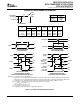
SN74LVC573A . . . RGY PACKAGE
(TOP VIEW)
1 20
10 11
2
3
4
5
6
7
8
9
19
18
17
16
15
14
13
12
1Q
2Q
3Q
4Q
5Q
6Q
7Q
8Q
1D
2D
3D
4D
5D
6D
7D
8D
LE
V
GND
CC
SN54LVC573A . . . J OR W PACKAGE
SN74LVC573A . . . DB, DGV, DW, N,
NS, OR PW PACKAGE
(TOP VIEW)
1
2
3
4
5
6
7
8
9
10
20
19
18
17
16
15
14
13
12
11
OE
1D
2D
3D
4D
5D
6D
7D
8D
GND
V
CC
1Q
2Q
3Q
4Q
5Q
6Q
7Q
8Q
LE
SN54LVC573A . . . FK PACKAGE
(TOP VIEW)
3 2 1 20 19
9 10 11 12 13
4
5
6
7
8
18
17
16
15
14
2Q
3Q
4Q
5Q
6Q
3D
4D
5D
6D
7D
2D
1D
OE
8Q
7Q 1Q
8D
GND
LE
V
CC
OE
DESCRIPTION/ORDERING INFORMATION
SN54LVC573A, SN74LVC573A
OCTAL TRANSPARENT D-TYPE LATCHES
WITH 3-STATE OUTPUTS
SCAS300R – JANUARY 1993 – REVISED SEPTEMBER 2005
• Operate From 1.65 V to 3.6 V • I
off
Supports Partial-Power-Down Mode
Operation
• Inputs Accept Voltages to 5.5 V
• Latch-Up Performance Exceeds 250 mA Per
• Max t
pd
of 6.9 ns at 3.3 V
JESD 17
• Typical V
OLP
(Output Ground Bounce) <0.8 V
• ESD Protection Exceeds JESD 22
at V
CC
= 3.3 V, T
A
= 25 ° C
– 2000-V Human-Body Model (A114-A)
• Typical V
OHV
(Output V
OH
Undershoot) >2 V at
V
CC
= 3.3 V, T
A
= 25 ° C – 200-V Machine Model (A115-A)
• Support Mixed-Mode Signal Operation on All – 1000-V Charged-Device Model (C101)
Ports (5-V Input/Output Voltage With 3.3-V xxxxx
V
CC
)
The SN54LVC573A octal transparent D-type latch is designed for 2.7-V to 3.6-V V
CC
operation, and the
SN74LVC573A octal transparent D-type latch is designed for 1.65-V to 3.6-V V
CC
operation.
These devices feature 3-state outputs designed specifically for driving highly capacitive or relatively
low-impedance loads. They are particularly suitable for implementing buffer registers, input/output (I/O) ports,
bidirectional bus drivers, and working registers.
While the latch-enable (LE) input is high, the Q outputs follow the data (D) inputs. When LE is taken low, the Q
outputs are latched at the logic levels at the D inputs.
A buffered output-enable ( OE) input can be used to place the eight outputs in either a normal logic state (high or
low logic levels) or the high-impedance state. In the high-impedance state, the outputs neither load nor drive the
bus lines significantly. The high-impedance state and increased drive provide the capability to drive bus lines
without interface or pullup components.
OE does not affect the internal operations of the latches. Old data can be retained or new data can be entered
while the outputs are in the high-impedance state.
These devices are fully specified for partial-power-down applications using I
off
. The I
off
circuitry disables the
outputs, preventing damaging current backflow through the device when it is powered down.
Please be aware that an important notice concerning availability, standard warranty, and use in critical applications of Texas
Instruments semiconductor products and disclaimers thereto appears at the end of this data sheet.
PRODUCTION DATA information is current as of publication date.
Copyright © 1993–2005, Texas Instruments Incorporated
Products conform to specifications per the terms of the Texas
On products compliant to MIL-PRF-38535, all parameters are
Instruments standard warranty. Production processing does not
tested unless otherwise noted. On all other products, production
necessarily include testing of all parameters.
processing does not necessarily include testing of all parameters.