
Datasheet


www.ti.com
DESCRIPTION/ORDERING INFORMATION (CONTINUED)
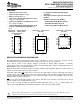
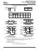
GQN OR ZQN PACKAGE
(TOP VIEW)
1 2 3 4
A
B
C
D
E
SN54LVC573A, SN74LVC573A
OCTAL TRANSPARENT D-TYPE LATCHES
WITH 3-STATE OUTPUTS
SCAS300R – JANUARY 1993 – REVISED SEPTEMBER 2005
To ensure the high-impedance state during power up or power down, OE should be tied to V
CC
through a pullup
resistor; the minimum value of the resistor is determined by the current-sinking capability of the driver.
Inputs can be driven from either 3.3-V or 5-V devices. This feature allows the use of these devices as translators
in a mixed 3.3-V/5-V system environment.
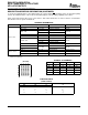
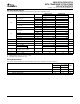
ORDERING INFORMATION
T
A
PACKAGE
(1)
ORDERABLE PART NUMBER TOP-SIDE MARKING
PDIP – N Tube of 20 SN74LVC573AN SN74LVC573AN
QFN – RGY Reel of 1000 SN74LVC573ARGYR LC573A
Tube of 25 SN74LVC573ADW
SOIC – DW LVC573A
Reel of 2000 SN74LVC573ADWR
SOP – NS Reel of 2000 SN74LVC573ANSR LVC573A
SSOP – DB Reel of 2000 SN74LVC573ADBR LC573A
–40 ° C to 85 ° C
Tube of 70 SN74LVC573APW
TSSOP – PW Reel of 2000 SN74LVC573APWR LC573A
Reel of 250 SN74LVC573APWT
TVSOP – DGV Reel of 2000 SN74LVC573ADGVR LC573A
VFBGA – GQN SN74LVC573AGQNR
Reel of 1000 LC573A
VFBGA – ZQN (Pb-free) SN74LVC573AZQNR
CDIP – J Tube of 20 SNJ54LVC573AJ SNJ54LVC573AJ
–55°C to 125°C CFP – W Tube of 85 SNJ54LVC573AW SNJ54LVC573AW
LCCC – FK Tube of 55 SNJ54LVC573AFK SNJ54LVC573AFK
(1) Package drawings, standard packing quantities, thermal data, symbolization, and PCB design guidelines are available at
www.ti.com/sc/package.
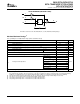
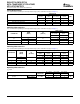
TERMINAL ASSIGNMENTS
1 2 3 4
A 1D OE V
CC
1Q
B 3D 3Q 2D 2Q
C 5D 4D 5Q 4Q
D 7D 7Q 6D 6Q
E GND 8D LE 8Q
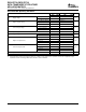
FUNCTION TABLE
(EACH LATCH)
INPUTS
OUTPUT
Q
OE LE D
L H H H
L H L L
L L X Q
0
H X X Z
2