
Datasheet


www.ti.com
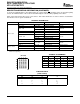
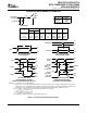
OE
To Seven Other Channels
1
11
2
19
LE
1D
C1
1D
1Q
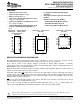
Pin numbers shown are for the DB, DGV, DW, FK, J, N, NS, PW, RGY, and W packages.
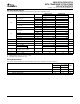
Absolute Maximum Ratings
(1)
SN54LVC573A, SN74LVC573A
OCTAL TRANSPARENT D-TYPE LATCHES
WITH 3-STATE OUTPUTS
SCAS300R – JANUARY 1993 – REVISED SEPTEMBER 2005
LOGIC DIAGRAM (POSITIVE LOGIC)
over operating free-air temperature range (unless otherwise noted)
MIN MAX UNIT
V
CC
Supply voltage –0.5 6.5 V
V
I
Input voltage range
(2)
–0.5 6.5 V
V
O
Voltage range applied to any output in the high-impedance or power-off state
(2)
–0.5 6.5 V
V
O
Voltage range applied to any output in the high or low state
(2) (3)
–0.5 V
CC
+ 0.5 V
I
IK
Input clamp current V
I
< 0 –50 mA
I
OK
Output clamp current V
O
< 0 –50 mA
I
O
Continuous output current ± 50 mA
Continuous current through V
CC
or GND ± 100 mA
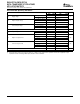
DB package
(4)
70
DGV package
(4)
92
DW package
(4)
58
GQN/ZQN package
(4)
78
θ
JA
Package thermal impedance ° C/W
N package
(4)
69
NS package
(4)
60
PW package
(4)
83
RGY package
(5)
37
T
stg
Storage temperature range –65 150 ° C
(1) Stresses beyond those listed under "absolute maximum ratings" may cause permanent damage to the device. These are stress ratings
only, and functional operation of the device at these or any other conditions beyond those indicated under "recommended operating
conditions" is not implied. Exposure to absolute-maximum-rated conditions for extended periods may affect device reliability.
(2) The input and output negative-voltage ratings may be exceeded if the input and output current ratings are observed.
(3) The value of V
CC
is provided in the recommended operating conditions table.
(4) The package thermal impedance is calculated in accordance with JESD 51-7.
(5) The package thermal impedance is calculated in accordance with JESD 51-5.
3