
Datasheet


www.ti.com
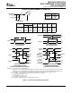
PARAMETER MEASUREMENT INFORMATION
V
M
t
h
t
su
From Output
Under Test
C
L
(see Note A)
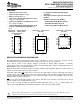
LOAD CIRCUIT
S1
V
LOAD
Open
GND
R
L
R
L
Data Input
Timing Input
V
I
0 V
V
I
0 V
0 V
t
w
Input
VOLTAGE WAVEFORMS
SETUP AND HOLD TIMES
VOLTAGE WAVEFORMS
PROPAGATION DELAY TIMES
INVERTING AND NONINVERTING OUTPUTS
VOLTAGE WAVEFORMS
PULSE DURATION
t
PLH
t
PHL
t
PHL
t
PLH
V
OH
V
OH
V
OL
V
OL
V
I
0 V
Input
Output
Waveform 1
S1 at V
LOAD
(see Note B)
Output
Waveform 2
S1 at GND
(see Note B)
V
OL
V
OH
t
PZL
t
PZH
t
PLZ
t
PHZ
V
LOAD
/2
0 V
V
OL
+ V
∆
V
OH
– V
∆
≈0 V
V
I
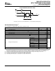
VOLTAGE WAVEFORMS
ENABLE AND DISABLE TIMES
LOW- AND HIGH-LEVEL ENABLING
Output
Output
t
PLH
/t
PHL
t
PLZ
/t
PZL
t
PHZ
/t
PZH
Open
V
LOAD
GND
TEST S1
NOTES: A. C
L
includes probe and jig capacitance.
B. Waveform 1 is for an output with internal conditions such that the output is low, except when disabled by the output control.
Waveform 2 is for an output with internal conditions such that the output is high, except when disabled by the output control.
C. All input pulses are supplied by generators having the following characteristics: PRR ≤ 10 MHz, Z
O
= 50 Ω.
D. The outputs are measured one at a time, with one transition per measurement.
E. t
PLZ
and t
PHZ
are the same as t
dis
.
F. t
PZL
and t
PZH
are the same as t
en
.
G. t
PLH
and t
PHL
are the same as t
pd
.
H. All parameters and waveforms are not applicable to all devices.
Output
Control
V
M
V
M
V
M
V
M
V
M
V
M
V
M
V
M
V
M
V
M
V
M
V
M
V
I
V
M
V
M
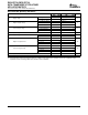
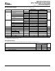
1.8 V ± 0.15 V
2.5 V ± 0.2 V
2.7 V
3.3 V ± 0.3 V
1 kΩ
500 Ω
500 Ω
500 Ω
V
CC
R
L
2 × V
CC
2 × V
CC
6 V
6 V
V
LOAD
C
L
30 pF
30 pF
50 pF
50 pF
0.15 V
0.15 V
0.3 V
0.3 V
V
∆
V
CC
V
CC
2.7 V
2.7 V
V
I
V
CC
/2
V
CC
/2
1.5 V
1.5 V
V
M
t
r
/t
f
≤2 ns
≤2 ns
≤2.5 ns
≤2.5 ns
INPUTS
SN54LVC573A, SN74LVC573A
OCTAL TRANSPARENT D-TYPE LATCHES
WITH 3-STATE OUTPUTS
SCAS300R – JANUARY 1993 – REVISED SEPTEMBER 2005
Figure 1. Load Circuit and Voltage Waveforms
7