
Datasheet


1
2
3
4
5
6
7
14
13
12
11
10
9
8
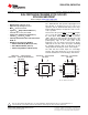
1CLR
1D
1CLK
1PRE
1Q
1Q
GND
V
CC
2CLR
2D
2CLK
2PRE
2Q
2Q
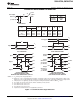
SN54LVC74A . . . J OR W PACKAGE
SN74LVC74A . . . D, DB, NS, OR PW PACKAGE
(TOP VIEW)
3 2 1 20 19
9 10 11 12 13
4
5
6
7
8
18
17
16
15
14
2D
NC
2CLK
NC
2PRE
1CLK
NC
1PRE
NC
1Q
1D
1CLR
NC
2Q
2Q
V
2CLR
1Q
GND
NC
SN54LVC74A . . . FK PACKAGE
(TOP VIEW)
CC
NC - No internal connection
SN74LVC74A . . . RGY PACKAGE
(TOP VIEW)
1 14
7 8
2
3
4
5
6
13
12
11
10
9
2CLR
2D
2CLK
2PRE
2Q
1D
1CLK
1PRE
1Q
1Q
1CLR
2Q
V
GND
CC
SN54LVC74A, SN74LVC74A
www.ti.com
SCAS287T –JANUARY 1993–REVISED JULY 2013
DUAL POSITIVE-EDGE-TRIGGERED D-TYPE FLIP-FLOPS
WITH CLEAR AND PRESET
Check for Samples: SN54LVC74A, SN74LVC74A
1
FEATURES
DESCRIPTION
The SN54LVC74A dual positive-edge-triggered D-
• Operate From 1.65 V to 3.6 V
type flip-flop is designed for 2.7-V to 3.6-V V
CC
• Inputs Accept Voltages to 5.5 V
operation, and the SN74LVC74A dual positive-edge-
• Max t
pd
of 5.2 ns at 3.3 V
triggered D-type flip-flop is designed for 1.65-V to 3.6-
V V
CC
operation.
• Typical V
OLP
(Output Ground Bounce)
<0.8 V at V
CC
= 3.3 V, T
A
= 25°C
A low level at the preset (PRE) or clear (CLR) inputs
sets or resets the outputs, regardless of the levels of
• Typical V
OHV
(Output V
OH
Undershoot)
the other inputs. When PRE and CLR are inactive
>2 V at V
CC
= 3.3 V, T
A
= 25°C
(high), data at the data (D) input meeting the setup
• Latch-Up Performance Exceeds 250 mA Per
time requirements is transferred to the outputs on the
JESD 17
positive-going edge of the clock pulse. Clock
• ESD Protection Exceeds JESD 22
triggering occurs at a voltage level and is not directly
related to the rise time of the clock pulse. Following
– 2000-V Human-Body Model (A114-A)
the hold-time interval, data at the D input can be
– 200-V Machine Model (A115-A)
changed without affecting the levels at the outputs.
– 1000-V Charged-Device Model (C101)
The data I/Os and control inputs are overvoltage
tolerant. This feature allows the use of these devices
for down-translation in a mixed-voltage environment.
1
Please be aware that an important notice concerning availability, standard warranty, and use in critical applications of
Texas Instruments semiconductor products and disclaimers thereto appears at the end of this data sheet.
PRODUCTION DATA information is current as of publication date.
Copyright © 1993–2013, Texas Instruments Incorporated
Products conform to specifications per the terms of the Texas
On products compliant to MIL-PRF-38535, all parameters are
Instruments standard warranty. Production processing does not
tested unless otherwise noted. On all other products, production
necessarily include testing of all parameters.
processing does not necessarily include testing of all parameters.