
Datasheet


Table Of Contents
www.ti.com
FEATURES
DESCRIPTION/ORDERING
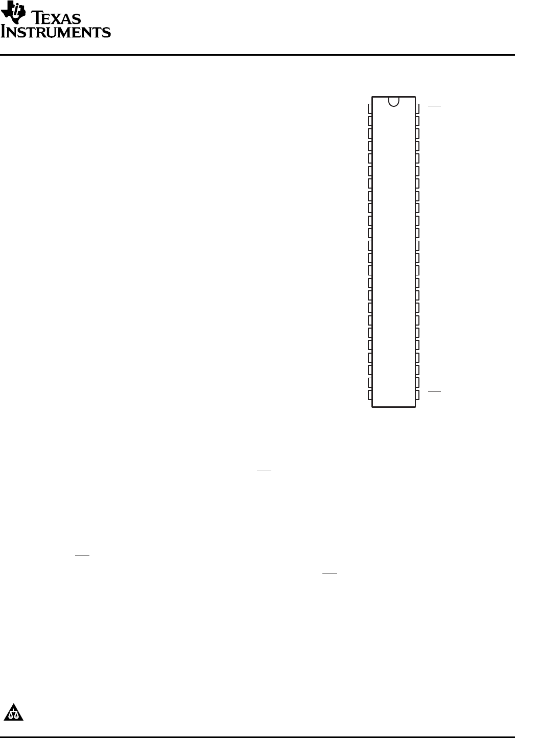
DGG, DGV, OR DL PACKAGE
(TOP VIEW)
1
2
3
4
5
6
7
8
9
10
11
12
13
14
15
16
17
18
19
20
21
22
23
24
48
47
46
45
44
43
42
41
40
39
38
37
36
35
34
33
32
31
30
29
28
27
26
25
1DIR
1B1
1B2
GND
1B3
1B4
V
CC
1B5
1B6
GND
1B7
1B8
2B1
2B2
GND
2B3
2B4
V
CC
2B5
2B6
GND
2B7
2B8
2DIR
1OE
1A1
1A2
GND
1A3
1A4
V
CC
1A5
1A6
GND
1A7
1A8
2A1
2A2
GND
2A3
2A4
V
CC
2A5
2A6
GND
2A7
2A8
2OE
This device can be used as two 8-bit transceivers or one 16-bit transceiver.
SN74LVCH16245A
16-BIT BUS TRANSCEIVER
WITH 3-STATE OUTPUTS
SCES495B – OCTOBER 2003 – REVISED AUGUST 2006
• Member of the Texas Instruments Widebus™
Family
• Operates From 1.65 V to 3.6 V
• Inputs Accept Voltages to 5.5 V
• Max t
pd
of 4 ns at 3.3 V
• Typical V
OLP
(Output Ground Bounce) <0.8 V
at V
CC
= 3.3 V, T
A
= 25 ° C
• Typical V
OHV
(Output V
OH
Undershoot) >2 V at
V
CC
= 3.3 V, T
A
= 25 ° C
• Supports Mixed-Mode Signal Operation on All
Ports (5-V Input/Output Voltage With
3.3-V V
CC
)
• I
off
Supports Partial-Power-Down Mode
Operation
• Bus Hold on Data Inputs Eliminates the Need
for External Pullup/Pulldown Resistors
• Latch-Up Performance Exceeds 250 mA Per
JESD 17
• ESD Protection Exceeds JESD 22
– 2000-V Human-Body Model (A114-A)
– 200-V Machine Model (A115-A)
INFORMATION
This 16-bit (dual-octal) noninverting bus transceiver
is designed for 1.65-V to 3.6-V V
CC
operation.
The SN74LVCH16245A is designed for asynchronous communication between data buses. The logic levels of
the direction-control (DIR) input and the output-enable ( OE) input activate either the B-port outputs or the A-port
outputs or place both output ports into the high-impedance mode. The device transmits data from the A bus to
the B bus when the B-port outputs are activated, and from the B bus to the A bus when the A-port outputs are
activated. The input circuitry on both A and B ports always is active and must have a logic HIGH or LOW level
applied to prevent excess I
CC
and I
CCZ
.
Active bus-hold circuitry holds unused or undriven data inputs at a valid logic state. Use of pullup or pulldown
resistors with the bus-hold circuitry is not recommended. The bus-hold circuitry is part of the input circuit and is
not disabled by OE or DIR.
To ensure the high-impedance state during power up or power down, OE should be tied to V
CC
through a pullup
resistor; the minimum value of the resistor is determined by the current-sinking capability of the driver.
Inputs can be driven from either 3.3-V or 5-V devices. This feature allows the use of these devices as translators
in a mixed 3.3-V/5-V system environment.
This device is fully specified for partial-power-down applications using I
off
. The I
off
circuitry disables the outputs,
preventing damaging current backflow through the device when it is powered down.
Please be aware that an important notice concerning availability, standard warranty, and use in critical applications of Texas
Instruments semiconductor products and disclaimers thereto appears at the end of this data sheet.
Widebus is a trademark of Texas Instruments.
PRODUCTION DATA information is current as of publication date.
Copyright © 2003–2006, Texas Instruments Incorporated
Products conform to specifications per the terms of the Texas
Instruments standard warranty. Production processing does not
necessarily include testing of all parameters.