
Datasheet


SCBS133F − MAY 1992 − REVISED OCTOBER 2003
1
POST OFFICE BOX 655303 • DALLAS, TEXAS 75265
D Supports Mixed-Mode Signal Operation
(5-V Input and Output Voltages With
3.3-V V
CC
)
D Supports Unregulated Battery Operation
Down to 2.7 V
D Typical V
OLP
(Output Ground Bounce)
<0.8 V at V
CC
= 3.3 V, T
A
= 25°C
D I
off
Supports Partial-Power-Down Mode
Operation
D Bus-Hold Data Inputs Eliminate the Need
for External Pullup Resistors
D Latch-Up Performance Exceeds 500 mA
Per JEDEC Standard JESD-17
D ESD Protection Exceeds JESD 22
− 2000-V Human-Body Model (A114-A)
− 200-V Machine Model (A115-A)
description/ordering information
This bus buffer is designed specifically for low-voltage (3.3-V) V
CC
operation, but with the capability to provide
a TTL interface to a 5-V system environment.
The SN74LVT125 features independent line drivers with 3-state outputs. Each output is in the high-impedance
state when the associated output-enable (OE
) input is high.
Active bus-hold circuitry holds unused or undriven inputs at a valid logic state. Use of pullup or pulldown resistors
with the bus-hold circuitry is not recommended.
This device is fully specified for partial-power-down applications using I
off
. The I
off
circuitry disables the outputs,
preventing damaging current backflow through the device when it is powered down.
To ensure the high-impedance state during power up or power down, OE
should be tied to V
CC
through a pullup
resistor; the minimum value of the resistor is determined by the current-sinking capability of the driver.
ORDERING INFORMATION
T
A
PACKAGE
†
ORDERABLE
PART NUMBER
TOP-SIDE
MARKING
SOIC − D
Tube SN74LVT125D
LVT125
SOIC − D
Tape and reel SN74LVT125DR
LVT125
−40°C to 85°C
SOP − NS Tape and reel SN74LVT125NSR LVT125
−40
°
C to 85
°
C
SSOP − DB Tape and reel SN74LVT125DBR LX125
TSSOP − PW
Tube SN74LVT125PW
LX125
TSSOP − PW
Tape and reel SN74LVT125PWR
LX125
†
Package drawings, standard packing quantities, thermal data, symbolization, and PCB design guidelines
are available at www.ti.com/sc/package.
Copyright 2003, Texas Instruments Incorporated
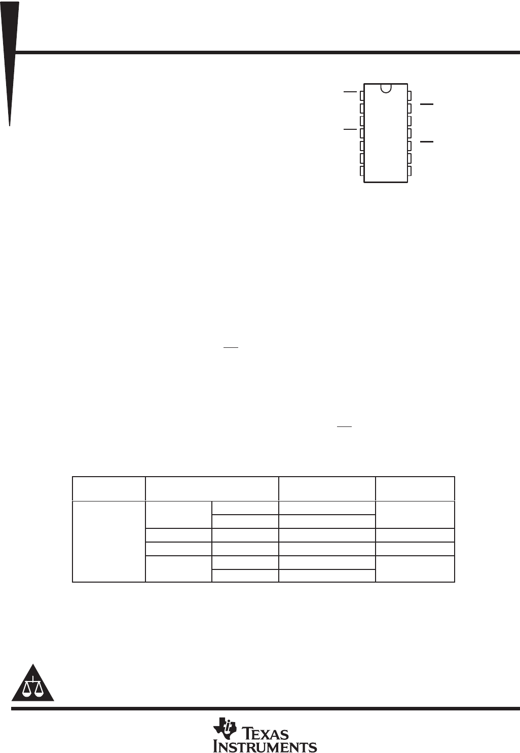
D, DB, NS, OR PW PACKAGE
(TOP VIEW)
1
2
3
4
5
6
7
14
13
12
11
10
9
8
1OE
1A
1Y
2OE
2A
2Y
GND
V
CC
4OE
4A
4Y
3OE
3A
3Y
Please be aware that an important notice concerning availability, standard warranty, and use in critical applications of
Texas Instruments semiconductor products and disclaimers thereto appears at the end of this data sheet.
!"#$ % &'!!($ #% )'*+&#$ ,#$(
!,'&$% &!" $ %)(&&#$% )(! $-( $(!"% (.#% %$!'"($%
%$#,#!, /#!!#$0 !,'&$ )!&(%%1 ,(% $ (&(%%#!+0 &+',(
$(%$1 #++ )#!#"($(!%