
Datasheet


SCAS352K − MARCH 1994 − REVISED OCTOBER 2003
1
POST OFFICE BOX 655303 • DALLAS, TEXAS 75265
D Support Mixed-Mode Signal Operation (5-V
Input and Output Voltages With 3.3-V V
CC
)
D Support Unregulated Battery Operation
Down to 2.7 V
D Typical V
OLP
(Output Ground Bounce)
<0.8 V at V
CC
= 3.3 V, T
A
= 25°C
D I
off
and Power-Up 3-State Support Hot
Insertion
D Bus Hold on Data Inputs Eliminates the
Need for External Pullup/Pulldown
Resistors
D Latch-Up Performance Exceeds 500 mA Per
JESD 17
D ESD Protection Exceeds JESD 22
− 2000-V Human-Body Model (A114-A)
− 200-V Machine Model (A115-A)
description/ordering information
These octal buffers/drivers are designed
specifically for low-voltage (3.3-V) V
CC
operation,
with the capability to provide a TTL interface to a
5-V system environment.
The ’LVTH241 devices are organized as two 4-bit
line drivers with separate output-enable (1OE
,
2OE) inputs. When 1OE
is low or 2OE is high, the
devices pass noninverted data from the A inputs
to the Y outputs. When 1OE
is high or 2OE is low,
the outputs are in the high-impedance state.
Active bus-hold circuitry holds unused or undriven inputs at a valid logic state. Use of pullup or pulldown resistors
with the bus-hold circuitry is not recommended.
ORDERING INFORMATION
T
A
PACKAGE
†
ORDERABLE
PART NUMBER
TOP-SIDE MARKING
SOIC − DW
Tube SN74LVTH241DW
LVTH241
SOIC − DW
Tape and reel SN74LVTH241DWR
LVTH241
−40°C to 85°C
SOP − NS Tape and reel SN74LVTH241NSR LVTH241
−40°C to 85°C
SSOP − DB Tape and reel SN74LVTH241DBR LXH241
TSSOP − PW
Tube SN74LVTH241PW
LXH241
TSSOP − PW
Tape and reel SN74LVTH241PWR
LXH241
CDIP − J Tube SNJ54LVTH241J SNJ54LVTH241J
−55°C to 125°C
CFP − W Tube SNJ54LVTH241W SNJ54LVTH241W
−55 C to 125 C
LCCC − FK Tube SNJ54LVTH241FK SNJ54LVTH241FK
†
Package drawings, standard packing quantities, thermal data, symbolization, and PCB design guidelines are
available at www.ti.com/sc/package.
Copyright 2003, Texas Instruments Incorporated
! "#$%&'( $#()(!
(*#+&)#( $%++'( )! #* ,%-.$)#( ")' +#"%$! $#(*#+& #
!,'$*$)#(! ,'+ ' '+&! #* '/)! (!+%&'(! !)(")+" 0)++)(1
+#"%$#( ,+#$'!!(2 "#'! (# ('$'!!)+.1 ($.%"' '!(2 #* )..
,)+)&''+!
Please be aware that an important notice concerning availability, standard warranty, and use in critical applications of
Texas Instruments semiconductor products and disclaimers thereto appears at the end of this data sheet.
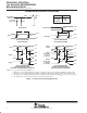
SN54LVTH241 ...J OR W PACKAGE
SN74LVTH241 . . . DB, DW, NS, OR PW PACKAGE
(TOP VIEW)
SN54LVTH241 . . . FK PACKAGE
(TOP VIEW)
1
2
3
4
5
6
7
8
9
10
20
19
18
17
16
15
14
13
12
11
1OE
1A1
2Y4
1A2
2Y3
1A3
2Y2
1A4
2Y1
GND
V
CC
2OE
1Y1
2A4
1Y2
2A3
1Y3
2A2
1Y4
2A1
3 2 1 20 19
9 10 11 12 13
4
5
6
7
8
18
17
16
15
14
1Y1
2A4
1Y2
2A3
1Y3
1A2
2Y3
1A3
2Y2
1A4
2Y4
1A1
1OE
1Y4
2A2
2OE
2Y1
GND
2A1
V
CC