
Datasheet


SCAS352K − MARCH 1994 − REVISED OCTOBER 2003
2
POST OFFICE BOX 655303 • DALLAS, TEXAS 75265
description/ordering information (continued)
When V
CC
is between 0 and 1.5 V, the devices are in the high-impedance state during power up or power down.
However, to ensure the high-impedance state above 1.5 V, OE
should be tied to V
CC
through a pullup resistor
and OE should be tied to GND through a pulldown resistor; the minimum value of the resistor is determined by
the current-sinking/current-sourcing capability of the driver.
These devices are fully specified for hot-insertion applications using I
off
and power-up 3-state. The I
off
circuitry
disables the outputs, preventing damaging current backflow through the devices when they are powered down.
The power-up 3-state circuitry places the outputs in the high-impedance state during power up and power down,
which prevents driver conflict.
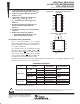
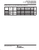
FUNCTION TABLES
INPUTS
OUTPUT
1OE 1A
OUTPUT
1Y
L H H
L LL
H X Z
INPUTS
OUTPUT
2OE 2A
OUTPUT
2Y
H H H
H LL
L X Z
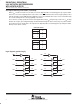
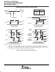
logic diagram (positive logic)
1
218
1Y1
1OE
1A1
416
1Y2
1A2
614
1Y3
1A3
812
1Y4
1A4
19
11 9
2Y1
2OE
2A1
13 7
2Y2
2A2
15 5
2Y3
2A3
17 3
2Y4
2A4