
Datasheet


SCAS352K − MARCH 1994 − REVISED OCTOBER 2003
3
POST OFFICE BOX 655303 • DALLAS, TEXAS 75265
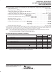
absolute maximum ratings over operating free-air temperature range (unless otherwise noted)
†
Supply voltage range, V
CC
−0.5 V to 4.6 V. . . . . . . . . . . . . . . . . . . . . . . . . . . . . . . . . . . . . . . . . . . . . . . . . . . . . . . . .
Input voltage range, V
I
(see Note 1) −0.5 V to 7 V. . . . . . . . . . . . . . . . . . . . . . . . . . . . . . . . . . . . . . . . . . . . . . . . . .
Voltage range applied to any output in the high-impedance
or power-off state, V
O
(see Note 1) −0.5 V to 7 V. . . . . . . . . . . . . . . . . . . . . . . . . . . . . . . . . . . . . . . . . . . . . . . .
Voltage range applied to any output in the high state, V
O
(see Note 1) −0.5 V to V
CC
+ 0.5 V. . . . . . . . . . . . .
Current into any output in the low state, I
O
: SN54LVTH241 96 mA. . . . . . . . . . . . . . . . . . . . . . . . . . . . . . . . . . .
SN74LVTH241 128 mA. . . . . . . . . . . . . . . . . . . . . . . . . . . . . . . . . .
Current into any output in the high state, I
O
(see Note 2): SN54LVTH241 48 mA. . . . . . . . . . . . . . . . . . . . . . .
SN74LVTH241 64 mA. . . . . . . . . . . . . . . . . . . . . . .
Input clamp current, I
IK
(V
I
< 0) −50 mA. . . . . . . . . . . . . . . . . . . . . . . . . . . . . . . . . . . . . . . . . . . . . . . . . . . . . . . . . . .
Output clamp current, I
OK
(V
O
< 0) −50 mA. . . . . . . . . . . . . . . . . . . . . . . . . . . . . . . . . . . . . . . . . . . . . . . . . . . . . . . .
Package thermal impedance, θ
JA
(see Note 3): DB package 70°C/W. . . . . . . . . . . . . . . . . . . . . . . . . . . . . . . . .
DW package 58°C/W. . . . . . . . . . . . . . . . . . . . . . . . . . . . . . . . .
NS package 60°C/W. . . . . . . . . . . . . . . . . . . . . . . . . . . . . . . . .
PW package 83°C/W. . . . . . . . . . . . . . . . . . . . . . . . . . . . . . . . .
Storage temperature range, T
stg
−65°C to 150°C. . . . . . . . . . . . . . . . . . . . . . . . . . . . . . . . . . . . . . . . . . . . . . . . . . .
†
Stresses beyond those listed under “absolute maximum ratings” may cause permanent damage to the device. These are stress ratings only, and
functional operation of the device at these or any other conditions beyond those indicated under “recommended operating conditions” is not
implied. Exposure to absolute-maximum-rated conditions for extended periods may affect device reliability.
NOTES: 1. The input and output negative-voltage ratings may be exceeded if the input and output clamp-current ratings are observed.
2. This current flows only when the output is in the high state and V
O
> V
CC
.
3. The package thermal impedance is calculated in accordance with JESD 51-7.
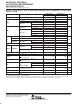
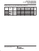
recommended operating conditions (see Note 4)
SN54LVTH241 SN74LVTH241
UNIT
MIN MAX MIN MAX
UNIT
V
CC
Supply voltage 2.7 3.6 2.7 3.6 V
V
IH
High-level input voltage 2 2 V
V
IL
Low-level input voltage 0.8 0.8 V
V
I
Input voltage 5.5 5.5 V
I
OH
High-level output current −24 −32 mA
I
OL
Low-level output current 48 64 mA
∆t/∆v Input transition rise or fall rate Outputs enabled 10 10 ns/V
∆t/∆V
CC
Power-up ramp rate 200 200 µs/V
T
A
Operating free-air temperature −55 125 −40 85 °C
NOTE 4: All unused control inputs of the device must be held at V
CC
or GND to ensure proper device operation. Refer to the TI application report,
Implications of Slow or Floating CMOS Inputs, literature number SCBA004.
(*#+&)#( $#($'+(! ,+#"%$! ( ' *#+&)3' #+
"'!2( ,)!' #* "'3'.#,&'( )+)$'+!$ ")) )(" #'+
!,'$*$)#(! )+' "'!2( 2#).! '/)! (!+%&'(! +'!'+3'! ' +2 #
$)(2' #+ "!$#((%' '!' ,+#"%$! 0#% (#$'