
Datasheet
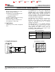


SN65220
,
SN65240
,
SN75240
SLLS266H –FEBRUARY 1997–REVISED MAY 2015
www.ti.com
8 Specifications
8.1 Absolute Maximum Ratings
over operating free-air temperature range (unless otherwise noted)
(1)
MIN MAX UNIT
P
D(peak)
Peak power dissipation 60 W
I
FSM
Peak forward surge current 3 A
I
RSM
Peak reverse surge current –9 A
T
stg
Storage temperature –65 150 °C
(1) Stresses beyond those listed under Absolute Maximum Ratings may cause permanent damage to the device. These are stress ratings
only, and functional operation of the device at these or any other conditions beyond those indicated under Recommended Operating
Conditions is not implied. Exposure to absolute-maximum-rated conditions for extended periods may affect device reliability.
8.2 ESD Ratings
VALUE UNIT
Human body model (HBM), per ANSI/ESDA/JEDEC JS-001, all pins
(1)
±15000
V
(ESD)
Electrostatic discharge V
Charged device model (CDM), per JEDEC specification JESD22-C101, all
±2000
pins
(2)
(1) JEDEC document JEP155 states that 500-V HBM allows safe manufacturing with a standard ESD control process.
(2) JEDEC document JEP157 states that 250-V CDM allows safe manufacturing with a standard ESD control process.
8.3 Recommended Operating Conditions
MIN MAX UNIT
SN75240 0 70
T
A
Ambient temperature °C
SN65220, SN65240 –40 85
8.4 Thermal Information
SN65220 SN65240, SN75240
DBV YZB P PW
THERMAL METRIC
(1)
UNIT
(SOT-23) (DSBGA) (PDIP) (TSSOP)
6 PINS 4 BALLS 8 PINS
R
θJA
Junction-to-ambient thermal resistance 199.5 170 67.5 185.3 °C/W
R
θJC(top)
Junction-to-case (top) thermal resistance 159.7 1.8 57.9 68.8 °C/W
R
θJB
Junction-to-board thermal resistance 51.1 43.5 44.5 114.0 °C/W
ψ
JT
Junction-to-top characterization parameter 41 9.2 36.2 9.9 °C/W
ψ
JB
Junction-to-board characterization parameter 50.5 43.5 44.5 112.3 °C/W
(1) For more information about traditional and new thermal metrics, see the Semiconductor and IC Package Thermal Metrics application
report, SPRA953.
8.5 Electrical Characteristics
over recommended operating conditions (unless otherwise noted)
PARAMETER TEST CONDITIONS MIN TYP MAX UNIT
I
lkg
Leakage current V
I
= 6 V at A, B, C, or D terminals 1 µA
V
(BR)
Breakdown voltage V
I
= 1 mA at A, B, C, or D terminals 6.5 7 8 V
C
IN
Input capacitance to ground V
I
= 0.4 sin (4E6πt) + 0.5 V 35 pF
4 Submit Documentation Feedback Copyright © 1997–2015, Texas Instruments Incorporated
Product Folder Links: SN65220 SN65240 SN75240