
Datasheet


SN65240
SN75240
GND
A
B
GND
GND
A
B
GND
GND
C
D
GND
SN65220
A,B,C or D
GND
D1
R1
Q1 D2
7.5
5
2.5
0
-2.5
-5
-7.5
-10
Current – A
-10
Voltage – V
-5 0 5 10 15
Measured
from A,B,C
or D to GND
V
BE
V
Z
V
FW
SN65220
,
SN65240
,
SN75240
SLLS266H –FEBRUARY 1997–REVISED MAY 2015
www.ti.com
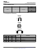
10 Detailed Description
10.1 Overview
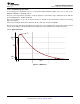
The SN65220, SN65240, and SN75240 devices integrate multiple unidirectional transient voltage suppressors
(TVS). Figure 4 shows the equivalent circuit diagram of a single TVS diode.
For positive transient voltages, only the Q1 transistor determines the switching characteristic. When the input
voltage reaches the Zener voltage, V
Z
, Zener diode D1 conducts; therefore, allowing for the base-emitter voltage,
V
BE
, to increase. At V
IN
= V
Z
+ V
BE
, the transistor starts conducting. From then on, its on-resistance decreases
linearly with increasing input voltage.
For negative transient voltages, only diode D2 determines the switching characteristic. Here, switching occurs
when the input voltage exceeds the diode forward voltage, V
FW
.
Figure 4. TVS Structure and Current — Voltage Characteristic
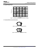
10.2 Functional Block Diagram
6 Submit Documentation Feedback Copyright © 1997–2015, Texas Instruments Incorporated
Product Folder Links: SN65220 SN65240 SN75240