
Datasheet


SLLS025A − JULY 1986
Copyright 1986, Texas Instruments Incorporated
Revision Information
3−1
POST OFFICE BOX 655303 • DALLAS, TEXAS 75265
POST OFFICE BOX 1443 • HOUSTON, TEXAS 77251−1443
• Dual Circuits Capable of Driving
High-Capacitance Loads at High Speeds
• Output Supply Voltage Range up to 24 V
• Low Standby Power Dissipation
description
The SN75372 is a dual NAND gate interface
circuit designed to drive power MOSFETs from
TTL inputs. It provides high current and voltage
levels necessary to drive large capacitive loads at
high speeds. The device operates from a V
CC1
of
5 V and a V
CC2
of up to 24 V.
The SN75372 is characterized for operation from
0°C to 70°C.
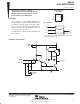
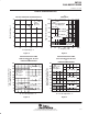
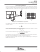
schematic (each driver)
V
CC1
V
CC2
To Other
Driver
To Other
Driver
Output Y
GND
Input A
Enable E
1Y
7
2Y
6
E
2
EN
1A
1
2A
3
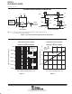
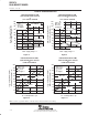
logic symbol
†
TTL/MOS
1
2
3
4
8
7
6
5
1A
E
2A
GND
V
CC1
1Y
2Y
V
CC2
D OR P PACKAGE
(TOP VIEW)
†
This symbol is in accordance with ANSI/IEEE Std 91-1984
and IEC Publication 617-12.
!"# $"%&! '#(
'"! ! $#!! $# )# # #* "#
'' +,( '"! $!#- '# #!#&, !&"'#
#- && $##(