
Datasheet


SN75468
,
SN75469
www.ti.com
SLRS023E –DECEMBER 1976–REVISED JANUARY 2015
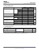
7.5 Electrical Characteristics
T
A
= 25°C (unless otherwise noted)
SN75468 SN75469
PARAMETER TEST CONDITIONS
(1)
UNIT
MIN TYP MAX MIN TYP MAX
I
C
= 125 mA
I
C
= 200 mA 2.4
I
C
= 250 mA 2.7
V
I(on)
On-state input voltage V
CE
= 2 V V
I
C
= 275 mA
I
C
= 300 mA 3
I
C
= 350 mA
I
I
= 250 µA, IC = 100 mA 0.9 1.1 0.9 1.1
V
CE(sat)
Collector-emitter saturation voltage I
I
= 350 µA, IC = 100 mA 1 1.3 1 1.3 V
I
I
= 500 µA, IC = 100 mA 1.2 1.6 1.2 1.6
V
F
Clamp-diode forward voltage I
F
= 350 mA 1.7 2 1.7 2 V
V
CE
= 100 V, I
I
= 0 50 50
I
CEX
collector cutoff current I
I
= 0 100 100 µA
V
CE
= 100 V,
TA = 70°C
V
I
= 1 V 500
I
I(off)
Off-state input current V
CE
= 50 V, I
C
= 500 µA, T
A
= 70°C 50 65 50 65 µA
V
I
= 3.85 V 0.93 1.35
I
I
Input current V
I
= 5 V 0.35 0.5 mA
V
I
= 12 V 1 1.45
V
R
= 100 V 50 50
I
R
Clamp-diode reverse current µA
V
R
= 100 V, T
A
= 70°C 100 10
C
i
Input Capacitance V
I
= 0, f = 1 MHz 15 25 15 25 pF
(1) All electrical characteristics are measured with 0.1-µF capacitors connected at REF, CT, and V
CC
to GND.
7.6 Switching Characteristics
T
A
= 25°C free-air temperature
PARAMETER TEST CONDITIONS
(1)
MIN TYP MAX UNIT
Propagation delay time, low-to-high-level
t
PLH
0.25 1 µs
output
V
S
= 20 V, R
L
= 163 Ω, C
L
= 15 pF,
See Figure 14
Propagation delay time, high-to-low-level
t
PHL
0.25 1 µs
output
V
S
= 50 V, I
O
= 300 mA, See
V
OH
High-level output voltage after switching V
S
– 20 mV
Figure 14
(1) All switching characteristics are measured with 0.1-µF capacitors connected at REF and V
CC
to GND.
Copyright © 1976–2015, Texas Instruments Incorporated Submit Documentation Feedback 5
Product Folder Links: SN75468 SN75469