
Datasheet


SN75468
,
SN75469
www.ti.com
SLRS023E –DECEMBER 1976–REVISED JANUARY 2015
9 Detailed Description
9.1 Overview
This standard device has proven ubiquity and versatility across a wide range of applications. This is due to its
integration of 7 Darlington transistors that are capable of sinking up to 500 mA and wide GPIO range capability.
The SN75468 comprises seven high voltage, high current NPN Darlington transistor pairs. All units feature a
common emitter and open collector outputs. To maximize their effectiveness, these units contain suppression
diodes for inductive loads. The SN75468 has a series base resistor to each Darlington pair, thus allowing
operation directly with TTL or CMOS operating at supply voltages of 5.0 V or 3.3 V. The SN75468 offers
solutions to a great many interface needs, including solenoids, relays, lamps, small motors, and LEDs.
Applications requiring sink currents beyond the capability of a single output may be accommodated by paralleling
the outputs.
This device can operate over a wide temperature range (–40°C to 105°C).
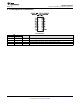
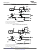
9.2 Functional Block Diagram
9.3 Feature Description
Each channel of SN75468 consists of Darlington connected NPN transistors. This connection creates the effect
of a single transistor with a very high current gain (β2). This can be as high as 10,000 A/A at certain currents.
The very high β allows for high output current drive with a very low input current, essentially equating to
operation with low GPIO voltages.
The GPIO voltage is converted to base current via the 2.7 kΩ resistor connected between the input and base of
the pre-driver Darlington NPN. The 7.2 kΩ & 3.0 kΩ resistors connected between the base and emitter of each
respective NPN act as pull-downs and suppress the amount of leakage that may occur from the input.
The diodes connected between the output and COM pin is used to suppress the kick-back voltage from an
inductive load that is excited when the NPN drivers are turned off (stop sinking) and the stored energy in the
coils causes a reverse current to flow into the coil supply via the kick-back diode.
In normal operation the diodes on base and collector pins to emitter will be reversed biased. If these diode are
forward biased, internal parasitic NPN transistors will draw (a nearly equal) current from other (nearby) device
pins.
9.4 Device Functional Modes
9.4.1 Inductive Load Drive
When the COM pin is tied to the coil supply voltage, SN75468 is able to drive inductive loads and supress the
kick-back voltage via the internal free wheeling diodes.
9.4.2 Resistive Load Drive
When driving a resistive load, a pull-up resistor is needed in order for SN75468 to sink current and for there to be
a logic high level. The COM pin can be left floating for these applications.
Copyright © 1976–2015, Texas Instruments Incorporated Submit Documentation Feedback 9
Product Folder Links: SN75468 SN75469