SPIO-4 Precision Signal-Path Controller Board Users' Guide December 2010
Table of Contents 1.0 SPIO-4 System Overview ...................................................................................................................... 3 1.0 SPIO-4 System Overview ...................................................................................................................... 3 1.1 SPIO-4 System Features................................................................................................................ 3 1.2 Packing List ........................................
1.0 SPIO-4 System Overview The SPIO-4 is one of several National Semiconductor digital controller/capture boards that are used by multiple evaluation systems. The objective of these software/hardware evaluation systems is to allow our customers to easily and accurately evaluate National’s signal-path devices in a lab setting. At the time of SPIO-4’s release, two different evaluation system software (GUIs) make use of this board: the WaveVision-5 and the Sensor AFE.
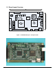
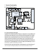
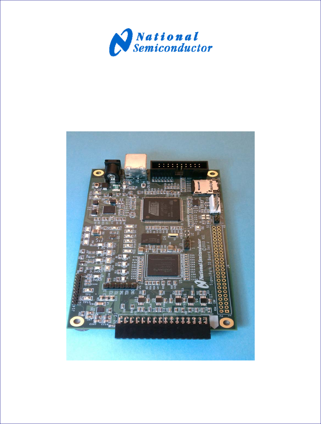
1.3 Board Layout Overview Figure 1 - SPIO-4 Board Layout – Component Side National Semiconductor Page 4 www.national.
1.4 Component Description The following table describes both the on-board connectors and the main components used in the SPIO-4 System shown in Figure 1. Component J1 J2 J3 J4 (DBG) J6 (GPSI-32) J7 (micro_SD) J8 (USB) J9 (JTAG) J10 (POWER) J14 (USNAP) JP1 U1 U4 U5 1.4.1.1 Description Serial Debug connector Header to provide access to the FPGA’s JTAG interface for debug Jumper to select J4 IO voltage (3.3V or programmable) Debug/Development Connector(See section 2.6). GPSI-16/32 Connector to DUT.
2 System Functionality 2.1 System Block Diagram Debug Connector(J1) Debug Connector(J9) 12MHZ Xtal 32kHZ Xtal GPSI 32 Connector (J6) SD Card (J7) > Level Shifters GPSI A GPSI A USB Connector (J8) GPIO Micro-Controller Atmel SAM3U (U1) USB GPSI A Pins 1,3,7,8,16 GPSI A Pins 5,6,9 DUT3.3V_EN < Level Shifters VDDIO I2C(SCL) Pin 12 I2C(SDA) Pin 11 DUT 3.3V DUT 5V Pin 13 Pin 14 3.3V_DUT NCS3/FPGA_CFG NCS2 USB 5V Pin 15 3.
2.3 Automatic Device Detection & Configuration The SPIO-4 system supports automatic hardware detection and configuration of the device under test. The GUI software actually carries out the device detection and configuration task. The FPGA is reconfigured on the fly by the host PC when the SPIO-4 Board is powered on, or whenever ADC evaluation boards are exchanged and SPIO-4 power is cycled. Each DUT board has either an FPGA configuration file, or a microcontroller firmware module, unique to it.
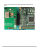
Below are two photos demonstrating the proper mating of a GPSI16 and a GPSI32 DUT board to the SPIO4. Figure 3 - GPSI 16 DUT to SPIO4 Mating National Semiconductor Page 8 www.national.
Figure 4 - GPSI 32 DUT to SPIO4 Mating 2.5.1 Level Shifters The board incorporates level shifters to allow flexible output voltages on the uni-directional SPI signals of GPSI-16 port, as shown in the board block diagram. VDDIO – a supply voltage from the GPSI-16/32 connector coming from the DUT board – provides the voltage to the output side of the level translators. If the DUT has no special requirements for voltage and simply needs basic 3.3V signal levels, the 3.
GPSI Connector (J6) Pin Description Pin Signal Name/Function # Pins 1-16 form the GPSI-16 subset: 1 2 3 4 5 6 7 8 9 10 11 12 13 14 SCS0_A~ SerialBus A – Chip Select for device 0. GND SCK_A Serial Bus A – Serial Clock from the master to the device. DUT_Present~ The DUT board shall ground this pin. The SPIO-4 senses this pin to determine the DUT board’s presence. SMISO_A Serial Bus A – Data from the slave (device) to the master.
15 16 17 18 19 20 21 22 23 the DUT board must leave this pin open. Maximum capacitor loading for this node is not to exceed 50uF. VDDIO Interface Supply always provided by the DUT board. Both the DUT board and the SPIO-4 board power their I/O drivers with this supply (except the I2C bus – which is always +3.3V). Only the SPI_A related signals on the GPSI-16 subset are affected by this I/O supply. Voltage Range: 1.6V to 5.5V. Capable of supplying 100mA. SCS2_A~ SerialBus A – Chip Select for device 2.
Serial Bus B – Data from the slave (device) to the master. The device may implement this as a tri-state signal that can be driven by multiple devices on Serial Bus B in a bussed fashion. The pull-up resistor, if required, is on the DUT board. 28 Available for implementation specific use. Refer to the DUT board manual. If unused, leave it open. 3.3V Available for implementation specific use. Refer to the DUT board manual. If unused, leave it open. 3.3V Available for implementation specific use.
3 SPIO-4 Bill of Materials Item 1 2 3 4 5 6 7 Description CAP CER 10000PF 25V Y5V 0603 CAP CER .47UF 10V X7R 0603 CAP .10UF 16V CERAMIC X7R 0603 Qty. 1 1 58 CAP CERAMIC 10PF 50V NP0 0603 CAP CER 15PF 50V C0G 5% 0603 CAP CER 4.7UF 10V Y5V 0603 CAP CER 10UF 6.3V Y5V 0603 2 4 5 22 8 9 10 11 12 13 14 15 16 17 18 19 20 21 22 23 24 25 26 27 28 29 30 31 32 33 CAP CER 1.0UF 10V X7R 0603 9 CAP CER 100UF 10V X5R 1210 3 CAP CER 10UF 10V X5R 0805 6 CAP CER 1.
4 SPIO-4 Schematics Following pages show the schematics of the board. These are provided for general information purposes only. National reserves the right to make modifications to the board design at any time. National Semiconductor Page 14 www.national.
BY USING THIS PRODUCT, YOU ARE AGREEING TO BE BOUND BY THE TERMS AND CONDITIONS OF NATIONAL SEMICONDUCTOR'S END USER LICENSE AGREEMENT. DO NOT USE THIS PRODUCT UNTIL YOU HAVE READ AND AGREED TO THE TERMS AND CONDITIONS OF THAT AGREEMENT. IF YOU DO NOT AGREE WITH THEM, CONTACT THE VENDOR WITHIN TEN (10) DAYS OF RECEIPT FOR INSTRUCTIONS ON RETURN OF THE UNUSED PRODUCT FOR A REFUND OF THE PURCHASE PRICE PAID, IF ANY.
8 7 6 5 4 3 2 1 SPIO45 Interface Board Block Diag E E D D C C B B A A National Semiconductor, Santa Clara, CA 95052 Title Size SPIO4 Block Diagram 2010 National Semiconductor Document Number B Date: 8 7 6 5 4 3 Rev 2.
8 7 6 5 4 3 2 1 Atmel ARM Microcontroller - Power, Debug, Analog 3p3V JP1 E JP U1B SAM3U VANA E C1 137 138 142 135 136 10nF 9 R1 RSTN DNS ERASE TEST JTAGSEL FWUP SHDN SW1 A B 39 VBG DGND DGND 11 NRST_PWR 9 9 9 9 9 9 D DHSD_P DHSD_M R2 R3 39R 39R DFSD_M DFSD_P 16 27 44 50 86 125 C5 10uF DGND VCORE DGND C6 0.1uF C7 0.1uF C8 0.1uF C9 0.1uF C10 0.1uF C11 0.1uF 17 51 85 104 127 VDDIO1 VDDIO2 VDDIO3 VDDIO4 VDDIO5 XIN XOUT C4 0.
8 7 6 5 4 3 2 1 Atmel ARM Microcontroller, Port Connection D[15:0] 4,5 D0 D1 D2 D3 D4 D5 D6 D7 D8 D9 D9 D11 D12 D13 D14 D15 U1A SAM3U E 9,11 VUSB_DET 8 CD 7 DUTCLKIN 8 CK 8 CDA 8 DA0 8 DA1 8 DA2 8 DA3 11 SDA 11 SCL CK CDA DA0 DA1 DA2 DA3 RXD_IN TXD_OUT 1 TP19 CD TP17 DUT_SDA 1 7 7 7 7 DUT_SCL CPUMISO_A CPU_MOSI_A CPU_SCLK_A CPU_CS0N_A USNAP_SCLK_N USNAP_MOSI USNAP_MISO D 11 11 ONSTAT USBISEL USNAP_SEL_N USNAP_IRQ_N TP4 1 TP7 7 DUT_SDA 7 DUT_SCL 5 SCC_TD 5 PCK 5 SCC_CLK 7 DUTDRD
5 4 3 2 1 D D 3,5 3,5 A[23:1] U4 A1 A2 A3 A4 A5 A6 A7 A8 A9 A10 A11 A12 A13 A14 A15 A16 A17 A18 A19 A20 A21 A22 A23 C B 3,5 3,5 3,5 3,5 NCS0 NRD NWE 3,5 3,5 NBS1 NBS0 A3 A4 A5 B3 B4 C3 C4 D4 H2 H3 H4 H5 G3 G4 F3 F4 E4 D3 H1 G2 H6 E3 J4 B5 A2 G5 B2 A1 A6 J3 J2 SRAM_CNTRL_REG A0 A1 A2 A3 A4 A5 A6 A7 A8 A9 A10 A11 A12 A13 A14 A15 A16 A17 A18 A19 A20 A21 A22 CS OE WE D[15:0] MT45W8MW16BGX DQ0 DQ1 DQ2 DQ3 DQ4 DQ5 DQ6 DQ7 DQ8 DQ9 DQ10 DQ11 DQ12 DQ13 DQ14 DQ15 WAIT RFU3 RFU4 B6 C5 C6 D5 E
5 3,4 4 2 1 D[15:0] D0 D1 D2 D3 D4 D5 D6 D7 D8 D9 D9 D11 D12 D13 D14 D15 D 3,4 3 U5-2 NOTE:D0-7 SWAPPED GOING INTO CONFIG BITS U5-3 D2 3 FPGA_INIT_N 3,4 NCS0 3,4 NWE 3,4 3,4 3,4 3,4 NRD NBS0 NBS1 NWAIT NCS0 D4 D15 D14 D13 D12 D11 D10 D9 D8 A[23:1] A1 A2 A3 A4 A5 A6 A7 A8 A9 A10 A11 A12 A13 A14 A15 A16 A17 A18 A19 A20 A21 A22 A23 C NRD NBS0 NBS1 NWAIT FPGA_CFG_CSN D5 D6 3 FPGA_M0 D3 3 NCS2 CCLK R15 3 D1 FPGA_CCLK DATA_D7_CFG_D0 FPGA_M1 2 CLK_12MHZ 3 PCK1 D0 R3 U3 T4 U5 T5 V7 U7 T7
5 4 3 2 1 XILINX JTAG HDR FOR CONFIG OR CHIPSCOPE 3p3V JUMER TO SELECT BANK VOUT 3p3V DGND DBG1 DBG3 DBG5 DBG7 DBG9 DBG11 DBG13 DBG15 DBG17 DBG19 DBG21 DBG23 DBG25 DBG27 DBG29 DBG31 DBG33 DBG35 DBG37 DBG39 DBG41 DBG43 DBG45 DBG47 1 3 5 7 9 11 13 15 17 19 21 23 25 27 29 31 33 35 37 39 41 43 45 47 49 2 4 6 8 10 12 14 16 18 20 22 24 26 28 30 32 34 36 38 40 42 44 46 48 50 DBG2 DBG4 DBG6 DBG8 DBG10 DBG12 DBG14 DBG16 DBG18 DBG20 DBG22 DBG24 DBG26 DBG28 DBG30 DBG32 DBG34 DBG36 DBG38 DBG40 DBG42 DBG44 DBG
5 4 3 2 1 3p3V DUT INPUT LEVEL SHIFTERS U6 8 1 VCCB VCCA DUT_VDDIO 7 6 REF_CLKA SDRDYN_A B1 B2 A1 A2 DIRA2B GND D 7 6 SMISO_A VCCB VCCA B1 B2 A1 A2 DIRA2B GND DUTCLKIN_R R14 33R DUTDRDYN_R 7 6 SCS1N_A_R R17 33R SCLK_A B1 B2 A1 A2 SCLK_A_R DIRA2B GND D 1 U5-1 DGND R15 33R 2 3 DUTMISO_A_R 5 4 CPUMISO_A_R DUTMISO_A CPUMISO_A 3 R53 0R RSTUFF OPTIONS TO SUPPORT CPU ONLY 8 R18 33R SCS0N_A 7 6 SCS0N_A_R R19 33R SMOSI_A VCCB VCCA B1 B2 A1 A2 SMOSI_A_R DIRA2B GND R20 33R
8 7 6 5 4 3 2 1 Micro SD Card E E 3p3V 3p3V R22 46.4K R21 10.0K R23 46.4K R24 46.4K 3p3V R25 46.4K R26 10.0K J7 D 3 3 3 DA2 DA3 CDA 3 CK 3 3 DA0 DA1 1 2 3 4 5 6 7 8 DA2 DA3 CDA CK DA0 DA1 DAT2 CD/DAT3 CMD VDD CLK VSS DAT0 DAT1 CD GND1 GND2 GND3 GND4 13 CD CD D 3 9 10 11 12 MICRO_SD DGND DGND C C 3p3V C74 0.
8 7 6 5 4 3 2 1 USB, CPU JTAG E E J8 USB TYPE B PORT R27 D 2 2 6 5 3 2 4 1 VUSB_RTN DHSD_P DHSD_M VUSB_DET 3,11 VUSB_DET 0R R28 46.4K 0R VUSB R29 68K C78 10pF C76 0.1uF C77 E_GND1 E_GND0 D+ DGND VBUS D VUSB_IN F1 4.7uF DGND DGND DGND DGND C C 3p3V R30 10.0K R31 10.0K R32 10.0K R33 10.0K R34 10.0K J9 IDC20-2.
8 7 6 5 4 3 2 1 E E D D C C B B A A National Semiconductor, Santa Clara, CA 95052 Title Size SPIO4 Power Block Diagram 2010 National Semiconductor Document Number B Date: 8 7 6 5 4 3 Rev 2.
8 7 6 5 4 3 2 1 3p3V 3.3V, 1.2V, 1.8V, DUT Power Supply out 7 21 22 36 VIN 5VIN C86 PTC_1A_1812 D12 DIODE ZENER 2 RING in 2 C38 4.7uF C39 10uF C87 10uF C82 10uF C83 10uF C84 10uF 4.7uF C85 0.1uF 46 42 41 DGND PJ037A DGND DGND 47 R44 1.5K 3p3V 45 VUSB R45 1.
IMPORTANT NOTICE Texas Instruments Incorporated and its subsidiaries (TI) reserve the right to make corrections, modifications, enhancements, improvements, and other changes to its products and services at any time and to discontinue any product or service without notice. Customers should obtain the latest relevant information before placing orders and should verify that such information is current and complete.