
VLYNQ Port User's Guide


www.ti.com
2 Peripheral Architecture
2.1 Clock Control
VLYNQ
CLKDIR=0
DMxxxdevice
VLYNQ_CLK
VLYNQ
CLKDIR=0
VLYNQdevice
VLYNQ
CLKDIR=1
DMxxxdevice
VLYNQ_CLK
VLYNQ
CLKDIR=1
VLYNQdevice
VLYNQ
internal
sysclk
Don’t
care
Peripheral Architecture
This section discusses the architecture and basic functions of the VLYNQ peripheral.
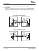
The module's serial clock direction and frequency are software configurable through the CLKDIR and
CLKDIV bits in the VLYNQ control register (CTRL). The VLYNQ serial clock can be sourced from the
internal system clock (CLKDIR = 1) or by an external clock source (CLKDIR = 0) for its serial operations.
The CLKDIV bit can divide the serial clock (1/1 - 1/8) down when the internal clock is selected as the
source. The serial clock is not affected by the CLKDIV bit values, if the serial clock is externally sourced.
The reset value of the CLKDIR bit is 0 (external clock source).
The external clock source is shown in Figure 2 . The internal clock source is shown in Figure 3 .
Figure 2. External Clock Block Diagram
Figure 3. Internal Clock Block Diagram
VLYNQ Port10 SPRU938B – September 2007
Submit Documentation Feedback