
VLYNQ Port User's Guide

www.ti.com
2.2 Signal Descriptions
2.3 Pin Multiplexing
2.4 Protocol Description
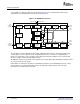
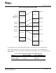
Peripheral Architecture
The VLYNQ module on the DM643x device supports 1 to 4 bit-wide RX/TX configurations. Chip-level pin
multiplexing registers control the configuration. See the pin multiplexing information in the device-specific
data manual.
If the VLYNQ data width does not match the number of transmit/receive lines that are available on the
remote device, negotiation between the two VLYNQ devices automatically configures the width (see
Section 2.7 ).
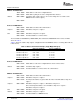
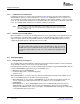
The VLYNQ interface signals are shown in Table 1 .
Table 1. VLYNQ Signal Descriptions
Pin Name Signal Name Signal Type Function
VLYNQ_CLOCK VLYNQ serial clock Input/Output The VLYNQ reference clock supports the internally or
externally generated clock.
VLYNQ_SCRUN VLYNQ serial clock run Input/Output The VLYNQ serial clock run request allows remote requests
request (Active low) for the VLYNQ serial clock to be turned off for system power
management.
Low: The request VLYNQ serial clock is active.
High: The VLYNQ serial clock is requested to be high when
all transactions are complete.
VLYNQ_RXD[0:3] VLYNQ receive data Input VLYNQ receive data is synchronous with the VLYNQ serial
clock.
VLYNQ_TXD[0:3] VLYNQ transmit data Output VLYNQ transmit data is synchronous with the VLYNQ serial
clock.
Extensive use of pin multiplexing is used to accommodate the largest number of peripheral functions in
the smallest possible package. Pin multiplexing is controlled using a combination of hardware
configurations at device reset and software programmable register settings. The VLYNQ module pins are
not enabled at reset. In order to change the default function of device pins at reset, the pin multiplexing
registers (PINMUX n) must be configured appropriately. Refer to the pin multiplexing information in the
device-specific data manual for more detailed information on the processor pin multiplexing and
configuration registers.
VLYNQ relies on 8b/10b block coding to minimize the number of serial pins and allows for in-band packet
delineation and control.
Appendix A provides general information on 8b/10b coding definitions and their implementation within the
VLYNQ module in the DM643x device.
SPRU938B – September 2007 VLYNQ Port 11
Submit Documentation Feedback