
Marine Instruments User Manual

www.ti.com
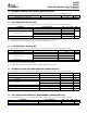
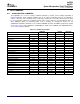
3.4 INTERNAL TEMPERATURE SENSOR CHARACTERISTICS
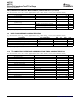
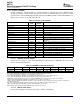
3.5 HIGH FREQUENCY OSCILLATOR
3.6 LOW FREQUENCY OSCILLATOR
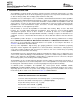
3.7 INTEGRATING ADC (COULOMB COUNTER) CHARACTERISTICS
3.8 ADC (TEMPERATURE AND CELL MEASUREMENT) CHARACTERISTICS
bq27500
bq27501
System-Side Impedance Track™ Fuel Gauge
SLUS785 – SEPTEMBER 2007
T
A
= –40 ° C to 85 ° C, 2.4 V < V
CC
< 2.6 V; Typical Values at T
A
= 25 ° C and V
CC
= 2.5 V (unless otherwise noted)
PARAMETER TEST CONDITIONS MIN TYP MAX UNIT
G
TEMP
Temperature sensor voltage gain –2.0 mV/ ° C
T
A
= –40 ° C to 85 ° C, 2.4 V < V
CC
< 2.6 V; Typical Values at T
A
= 25 ° C and V
CC
= 2.5 V (unless otherwise noted)
PARAMETER TEST CONDITIONS MIN TYP MAX UNIT
f
OSC
Operating frequency 2.097 MHz
T
A
= 0 ° C to 60 ° C –2.0% 0.38% 2.0%
f
EIO
Frequency error
(1) (2)
T
A
= –20 ° C to 70 ° C –3.0% 0.38% 3.0%
T
A
= –40 ° C to 85 ° C –4.5% 0.38% 4.5%
t
SXO
Start-up time
(3)
2.5 5 ms
(1) The frequency error is measured from 2.097 MHz.
(2) The frequency drift is included and measured from the trimmed frequency at V
CC
= 2.5V, T
A
= 25 ° C.
(3) The startup time is defined as the time it takes for the oscillator output frequency to be ± 3%.
T
A
= –40 ° C to 85 ° C, 2.4 V < V
CC
< 2.6 V; Typical Values at T
A
= 25 ° C and V
CC
= 2.5 V (unless otherwise noted)
PARAMETER TEST CONDITIONS MIN TYP MAX UNIT
f
LOSC
Operating frequency 32.768 kHz
T
A
= 0 ° C to 60 ° C –1.5% 0.25% 1.5%
f
LEIO
Frequency error
(1) (2)
T
A
= –20 ° C to 70 ° C –2.5% 0.25% 2.5%
T
A
= –40 ° C to 85 ° C –4.0% 0.25% 4.0%
t
LSXO
Start-up time
(3)
500 μ s
(1) The frequency drift is included and measured from the trimmed frequency at V
CC
= 2.5V, T
A
= 25 ° C.
(2) The frequency error is measured from 32.768 kHz.
(3) The startup time is defined as the time it takes for the oscillator output frequency to be ± 3%.
T
A
= –40 ° C to 85 ° C, 2.4 V < V
CC
< 2.6 V; Typical Values at T
A
= 25 ° C and V
CC
= 2.5 V (unless otherwise noted)
PARAMETER TEST CONDITIONS MIN TYP MAX UNIT
V
SR_IN
Input voltage range, V
(SRN)
and V
(SRP)
V
SR
= V
(SRN)
– V
(SRP)
–0.125 0.125 V
t
SR_CONV
Conversion time Single conversion 1 s
Resolution 14 15 bits
Before calibration 1 mV
V
SR_OS
Input offset
After calibration 10 μ V
INL Integral nonlinearity error ± 0.007 ± 0.034 % FSR
Z
SR_IN
Effective input resistance
(1)
2.5 M Ω
I
SR_LKG
Input leakage current
(1)
0.3 μ A
(1) Specified by design. Not tested in production.
T
A
= –40 ° C to 85 ° C, 2.4 V < V
CC
< 2.6 V; Typical Values at T
A
= 25 ° C and V
CC
= 2.5 V (unless otherwise noted)
PARAMETER TEST CONDITIONS MIN TYP MAX UNIT
V
ADC_IN
Input voltage range –0.2 1 V
Submit Documentation Feedback ELECTRICAL SPECIFICATIONS 5