Data Manual February 2004 Digital Audio Solutions SLES038C
Contents Section 1 2 3 Title Page Introduction . . . . . . . . . . . . . . . . . . . . . . . . . . . . . . . . . . . . . . . . . . . . . . . . . . . . . . . 1−1 1.1 Features . . . . . . . . . . . . . . . . . . . . . . . . . . . . . . . . . . . . . . . . . . . . . . . . . . . . 1−1 1.2 Terminal Assignments . . . . . . . . . . . . . . . . . . . . . . . . . . . . . . . . . . . . . . . . . 1−2 1.3 Hardware Block Diagram . . . . . . . . . . . . . . . . . . . . . . . . . . . . . . . . . . . . . . 1−3 1.
4 iv 3.6.1 Soft Volume . . . . . . . . . . . . . . . . . . . . . . . . . . . . . . . . . . . . . . . . 3−17 3.6.2 Loudness Compensation . . . . . . . . . . . . . . . . . . . . . . . . . . . . 3−24 3.6.3 Time Alignment and Reverb Delay Processing . . . . . . . . . . 3−26 3.7 Dynamic Range Control (DRC) . . . . . . . . . . . . . . . . . . . . . . . . . . . . . . . . 3−29 3.7.1 DRC Implementation . . . . . . . . . . . . . . . . . . . . . . . . . . . . . . . . 3−31 3.7.
List of Illustrations Figure Title Page 2−1 TAS3103 Detailed Hardware Block Diagram . . . . . . . . . . . . . . . . . . . . . . . . . . . 2−2 2−2 Discrete Serial Data Formats . . . . . . . . . . . . . . . . . . . . . . . . . . . . . . . . . . . . . . . . 2−3 2−3 Four-Channel TDM Serial Data Formats . . . . . . . . . . . . . . . . . . . . . . . . . . . . . . 2−3 2−4 SAP Configuration Subaddress Fields . . . . . . . . . . . . . . . . . . . . . . . . . . . . . . . .
3−10 TAS3103 3D Effects Processing Block . . . . . . . . . . . . . . . . . . . . . . . . . . . . . . . 3−9 3−11 Biquad Filter Structure and Coefficient Subaddress Format . . . . . . . . . . . . 3−10 3−12 Bass and Treble Filter Selections . . . . . . . . . . . . . . . . . . . . . . . . . . . . . . . . . . 3−12 3−13 Bass and Treble Application Example—Subaddress Parameters . . . . . . . 3−14 3−14 I2C Bass/Treble Activity Monitor Procedure . . . . . . . . . . . . . . . . . . . . . . . . .
List of Tables Table Title 2−1 TAS3103 Throughput Latencies vs MCLK and LRCLK . . . . . . . . . . . . . . . . . 2−2 TAS3103 Clock Default Settings . . . . . . . . . . . . . . . . . . . . . . . . . . . . . . . . . . . . 2−3 I2C EEPROM Data . . . . . . . . . . . . . . . . . . . . . . . . . . . . . . . . . . . . . . . . . . . . . . . . 2−4 Four Byte Write Exceptions—Reserved and Factory-Test I2C Subaddresses . . . . . . . . . . . . . . . . . . . . . . . . . . . . . . . . . . . . . . . . . . . . . . . . . .
viii
1 Introduction The TAS3103 is a fully configurable digital audio processor that preserves high-quality audio by using a 48-bit data path, 28-bit filter coefficients, and a single cycle 28 x 48-bit multiplier and 76-bit accumulator. Because of the coefficient-configurable fixed-program architecture of the TAS3103, a complete set of user-specific audio processing functions can be realized, with short development times, in a small, low power, low-cost device.
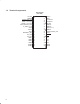
1.2 Terminal Assignments DBT PACKAGE (TOP VIEW) SCLKIN PWRDN REGULATOR_EN XTALI (1.8-V logic) XTALO (1.8-V logic) AVDD_BYPASS_CAP A_VDDS (3.3 V) AVSS MCLKI TEST MICROCLK_DIV I2C_SDA I2C_SCL SDIN1 SDIN2 SDIN3 SDIN4 GPIO0 GPIO1 1−2 1 38 2 37 3 36 4 35 5 34 6 33 7 32 8 31 9 30 10 29 11 28 12 27 13 26 14 25 15 24 16 23 17 22 18 21 19 20 LRCLK ORIN SCLKOUT2 SCLKOUT1 MCLKO SDOUT3 SDOUT2 VDDS (3.
1.
1−4 SDIN4 SDIN3 SDIN2 SDIN1 XTALO MCLKI XTALI MultiMode Serial to PCM Input Port Input Crossbar Mixer Oscillator PLL0 MultiMode 3D Effects Block PLL and Dividers Ch3 Ch2 Ch1 I2C_ PLL1 MC/Div SDA 1.
1.5 Ordering Information TA PLASTIC 38-PIN TSSOP (DBT) 0°C to 70°C TAS3103DBT −40°C to 85°C TAS3103IDBT 1.6 Terminal Functions TERMINAL NAME NO. I/O TYPE(1) DESCRIPTION PULLUP/ DOWN(2) A_VDDS (3.3 V) 7 PWR The PWR pin is used to input 3.3-V power to the DPLL and clock oscillator. This pin can be connected to the same power source used to drive the DVSS power pin. To achieve low DPLL jitter, this pin should be bypassed to AVSS with a 0.01-µF capacitor (low ESR preferable).
TERMINAL PULLUP/ DOWN(2) NO. I/O TYPE(1) DESCRIPTION I2C_SCL 13 I/O D I2C_SCL is the I2C clock pin. When the TAS3103 I2C port is a master, I2C_SCL is (1/2N) x (1/(M+1)) x 1/10 times the microprocessor clock, where N and M are set to 2 and 8 respectively. When the TAS3103 I2C port is a slave, input clock rates up to 400 kHz can be supported. This pin must be provided an external pullup (5 kΩ is recommended for most applications).
TERMINAL DESCRIPTION PULLUP/ DOWN(2) NO. I/O TYPE(1) PWRDN 2 I D PWRDN powers down all logic and stops all clocks whenever logic high is applied. However, the coefficient memory remains stable through a power down cycle, as long as a reset is not sent after a power down cycle. REGULATOR_EN 3 I D REGULATOR_EN is only used in factory tests. This pin should always be tied to ground. RST 26 I D RST is the master reset input. Applying a logic low to this pin generates a master reset.
TERMINAL PULLUP/ DOWN(2) NO. I/O TYPE(1) DESCRIPTION VDDS (3.3 V) 31 - PWR VDDS is the 3.3-V pin that powers (1) the 1.8-V internal power regulator used to supply logic power to the chip and (2) the I/O ring. It is recommended that this pin be bypassed to DVSS (pin 28) with a low ESR capacitor in the range of 0.01 µF. None XTALI (1.8-V logic) 4 I A XTALO and XTALI provide a master clock for the TAS3103 via use of an external fundamental mode crystal. XTALI is the 1.
1.7.1 Terminal-Controlled Modes 1.7.1.1 Clock Control MCLKI PLL1 PLL0 0 0 DAP CLOCK 11 x MCLK 0 1 (11 x MCLK)/2 1 0 (11 x MCLK)/4 1 1 MCLK (PLL bypass) MICROCLK_DIV MICROPROCESSOR CLOCK 0 DAP clock/4 1 DAP clock XTALI PLL0 PLL1 MICROCLK_DIV MCLK Reference Divider Microprocessor Scaler PLL ÷ 11 Digital Audio Processor (DAP) Clock 1400 x Fs 3 DAP Clock 3 136 MHz Microprocessor Clock < 36 MHz 1.7.1.
1−10 Slave Addr S Slave Addr Slave Addr S Slave Addr Ack m s xxxxxxx b Ack xxxxxxxx Ack xxxxxxxx Ack xxxxxxxx xxxxxxxx xxxxxxxx xxxxxxxx xxxxxxxx xxxxxxxx Ack Ack Ack Ack Ack Ack Ack Ack Ack Ack xxxxxxxx Ack Ack Ack xxxxxxxx xxxxxxxx 0x4E Channel 3 xxxxxxxx 0x4D Channel 2 Ack 0x4C Channel 1 m Ack Sub-Addr Ack 0000 s xxx b m 0000 s xxx b Subaddress xxxxxxxx xxxxxxxx xxxxxxxx xxxxxxxx xxxxxxxx Reverberation Block Reverberation Block Gains m Ack Sub-Addr Ack
1−11 S xxxxxxxx xxxxxxxx xxxxxxxx xxxxxxxx Ack Ack Ack Ack Ack Ack Ack Ack Ack xxxxxxxx xxxxxxxx Ack Ack Channel 3 = 0x75 Channel 2 = 0x74 Channel 1 = 0x73 Ack Ack xxxxxxxx l s b l s b l s b l s b l s b b0 b1 Ack Ack b2 a2 Ack Ack a1 Ack Ack Inline Gain Ack Bypass Gain Ack xxxxxx Ack xxxxxx Ack xxxxxx Ack xxxxxx Ack xxxxxx l Ack xxxxxx s b l Ack xxxxxx s b xxxxxxxx xxxxxxxx xxxxxxxx xxxxxxxx xxxxxxxx xxxxxxxx Bass and Treble Gain Coefficients xxxxxxxx 0x67
1−12 CH3 CH2 0x7B = Mix n to m 0x78 = Mix w to m 0x7A = Mix l to k 0x77 = Mix v to k 0x79 = Mix j to i Ack xxxxxxxx CH 3 Bass and Treble Block Mix_w_to_m CH 2 Bass and Treble Block Σ w Σ CH 2 Soft Volume CH 3 Soft Volume Σ l Mix_l_to_k Σ n Mix_n_to_m Σ o DRC_bypass_3 Σ q Mix_n_to_q_via_DRC_mult DRC_bypass_2 Σ p Mix_l_to_p_via_DRC_mult Mix_j_to_o_via_DRC_mult DRC_bypass_1 CH3 CH2 CH1 m S Slave Addr Ack Sub-Addr Ack 0000 s xxx b m 0000 s xxx b Mix_j_to_i Dynamic Range
1−13 Slave Addr Ack xxxxxxxx Ack xxxxxxxx l Ack xxxxxx s b Ack xxxxxxxx Ack xxxxxxxx 0x82 = Mix Channel 3 Output to o − 28-Bit Coefficient 0x83 = Mix Channel 3 Output to p − 28-Bit Coefficient m Ack Sub-Addr Ack 0000 s xxx b Ack Ack l Ack xxxxxx s b Channel 3 to Channel 1 and Channel 2 Mix Gain Coefficients 0x7F = Mix Dither 1 to o − 28-Bit Coefficient 0x80 = Mix Dither 2 to p − 28-Bit Coefficient 0x81 = Mix Dither 3 to q − 28-Bit Coefficient m Ack Sub-Addr Ack 0000 s xxx b Slave Addr Cha
1−14 Volume Commands I2C Bus Slave Addr Ack Sub-Addr Ack 0xF2 CH1 S S xxxxxxxx Ack xxxxxxxx CCC Ack xxxxxxxx Ack xxxxx HHH Ack 321 Ack xxxxxxxx l Ack xxxxxxx s Ack b ttransition Commanded Volume 48 AUDIO IN = x16 BoostMAX Volume Command = 1/223 Cut MAX (LSB) (5.
1−15 Audio Input CH2 Audio Input CH1 or CH3 5.23 Format RMS Voltage Estimator 32 Comparator T2-LSBits 25.23 Format 1−ae ae O1 { T1 O2 T2 { tWindow ≈ −1/[FS x ln(1−ae)] Where FS = Audio Sample Frequency CH1/CH2 = 0xB4 CH3 = 0xB9 CH1/CH2 = 0xB3 CH3 = 0xB8 25.
1−16 Slave Addr m Ack Sub-Addr Ack 0000 s b m 0000 s b m 0000 s b m 0000 s b m 0000 s b xxxxxxxx xxxxxxxx xxxxxxxx xxxxxxxx xxxxxxxx xxx Ack xxx Ack xxx Ack xxx Ack xxx Ack Slave Addr m Ack Sub-Addr Ack 0000 s xxx Ack b m 0000 s xxx Ack b S VU Meter Output = 0xFE S Slave Addr Slave Addr Ack Sub-Addr Ack Ack Sub-Addr Ack Ack Ack Ack Ack Ack xxxxx.xxx xxxxx.xxx xxxxx.xxx xxxxx.xxx xxxxx.xxx Ack Ack xxxxx.xxx xxxxx.xxx Ack xxxxx.xxx Ack Ack xxxxx.xxx xxxxx.xxx Ack xxxxx.
1−17 Σ Σ Σ Dither 1 Dither 2 Dither 3 Slave Addr Slave Addr Ack Ack xxxxxxxx xxxxxxxx Ack Sub-Addr Ack St6 St5 St4 St3 St2 St 1 p 00000000 Sampler xxxxxxxx xxxxxxxx 0.5 Ack 0xC7 0.
1−18 GPIO3 GPIO2 GPIO1 GPIO0 PWRDN S Slave Addr Ack LRCLK Sub-Addr 24 0xEF 16 15 8 7 0 D D D D Q Q Q Q Sample Logic LD Reset S Slave Addr Ack Reset 31 24 23 0xEE 16 15 Microprocessor Control Decode 216 8 23 16 15 8 7 0 7 0 3 2 1 0 Ack 4 3 GPIO_in_out Microprocessor Clock 1 (Default State) Disables Watchdog Timer Ack 00000000 Ack 00000000 Ack 00000000 Ack 0000000x Ack Watchdog Counter Sub-Addr 0xEB 31 24 Determines How Many Consecutive Logic 0 Samples (Whe
1−19 S Slave Addr Bass Filter Set N Ack Sub-Addr Ack 0xF2−0xF4—See Subaddress 0xA2 tTransition = TBLC[7:0] x 1/LRCLK 0xF1 24 00000000 31 Ack 16 8 xxxxxxxx 0 Ack CH1−CH3 Volume CMDS tTransition = TBLC[7:0] x 1/LRCLK Treble and Bass Slew Rate TBLC[7:0] v Ack 0000000 s Ack c 15 Treble Filter Set N 00000000 23 7 Master Mute/Un-Mute 0xF0—See Subaddress 0xA2 0xF1—Also See Subaddress 0xA2 and Subaddress 0xF5 Reserved/Factory Test Subaddresses GPIO Port I/O Values and GPIO Parameters 0xEC−
Subaddress—Bass and Treble Shelf Filter Parameters Treble/Bass Slew Rate Selection S 0xF1 Slave Addr 7 Ack Sub-Addr Ack CH3 CH2 00000000 Ack 00000000 V Ack 0000000 C Ack S S Slave Addr Ack Sub-Addr Ack 00000000 Ack 00000xxx Ack 00000xxx Ack 00000xxx xxxxxxxx Ack Treble/Bass Slew Rate = TBLC (Slew Rate = TBLC/FS, Where FS = Audio Sample Rate) CH1 Bass Filter Set Selection 0xF5 0 Ack CH2 CH3 CH1 Treble Filter Set Selection S 0xF7 Slave Addr Ack Sub-Addr Ack CH3 CH2 0000000
Master SCL I2C ÷10 1/(M+1) 3 2 ÷4 0 m[3:0] n[2:0] 6 MUX 1 0 MICROCLK_DIV MUX 0 1 2 3 MUX 7 6 5 ÷512 SCLKOUT2 MUX 1 SCLKOUT1 MUX 0 MUX 7 6 5 ÷16 ÷32 ÷8 4 ÷4 ÷256 ÷384 3 4 2 ÷2 1 0 ÷192 1 27 26 24 ÷4 ÷2 XTALI SCLKIN MUX 0 1 ICS 23 0xF9 w[1:0] y[2:0] Ack 28 ÷128 0 ÷2 ÷4 0 1 2 3 MUX MCLKO 3 ÷32 ÷64 29 MUX 0 1 2 PLL[1:0] PLL0 000 31 PLL BYPASS x11 PLL PLL1 2 1 0 NOTE: F9 must not be updated without first muting all three monaural channels in
Delay/Reverb Assignments 0xFA Delay S Delay Channel 1 = 2 x {D1[11:0] + 1} Slave Addr Reverb m l m l Ack Sub-Addr Ack 0000 s xxx Ack xxxxxxx s Ack 0000 s xxx Ack xxxxxxx s Ack D1 and R1 b b b b l m l m 0000 s xxx Ack xxxxxxx s Ack 0000 s xxx Ack xxxxxxx s Ack D2 and R2 b b b b l m l m 0000 s xxx Ack xxxxxxx s Ack 0000 s xxx Ack xxxxxxx s Ack D3 and R3 b b b b Note: 2 x (D1 + D2 + D3) + 3 x (R1 +R2 +R3) ≤ 4076 Delay Channel 2 = 2 x {D2[11:0] + 1} Delay Channel 3 = 2 x {D3[11:0] + 1} Reserved Reverb
SUB-ADDRESS(ES) 0xFC—See Subaddress 0x00 PARAMETER(S) Ending I2C Check Word 0xFD−0xFE—See Subaddress 0xBB Spectrum Analyzer/VU Meter Ouputs 0xFF—Volume Busy Flag Volume Flag S Slave Addr Ack Sub-Addr Ack 0000000x S S Volume Flag = 0 ⇒ No volume commands are active. Volume Flag = 1 ⇒ One or more volume commands are active.
1−24
2 Hardware Architecture Figure 2−1 depicts the hardware architecture of the chip.
SCLKIN MCLKI XTALI XTALO MCLKO ÷2 PLL1 PLL0 SCLKOUT1 ÷2 M U X MCLK ÷Z M U X ÷2 M U X PLL (x11) ÷4 M U X M U X ÷X M U X ÷Y SDIN1 MICROCLK_DIV SCLKOUT2 M U X OSC ÷2 LRCLK ORIN PLL and Clock Management 32 Bits SDOUT1 32 Bits 4K x 16 Delay Line RAM 32 Bits Dual Port Data RAM Coefficient RAM Program ROM 256 Bits 32 Bits Arithmetic Engine SDIN2 DAP Instruction Decoder/Sequencer SDOUT2 76-Bit Adder 32 Bits SDIN3 Regs Regs Digital Audio Processor (DAP) Arithmetic Unit 64 Bi
2.1 Input and Output Serial Audio Ports (SAPs) The TAS3103 accepts data in various serial data formats including left/right justified and I2S, 16 through 32 bits, discrete, or TDM. Sample rates from 8 kHz through 96 kHz are supported. Each TAS3103 has four input serial ports and three output serial ports, labeled SDIN[4:1] and SDOUT[3:1] respectively. All ports accommodate stereo data formats, and SDIN1 and SDOUT1 also accommodate time-division multiplex (TDM) data formats.
A 16-bit field contained in the 32-bit word located at I2C subaddress 0xF9 configures both the input and output serial audio ports. Figure 2−4 illustrates the format of this 16-bit field. The data is shown in the transmitted I2C protocol format, and thus, in addition to the data, the start bit S, the slave address, the subaddress, and the acknowledges required by every byte are also shown.
Enter Yes Vol Busy No Issue Mute Command Yes Vol Busy No Issue SAP Configuration Change Command Issue Un-Mute Command Yes Vol Busy No Mute Command = 0x00000007 at subaddress x0F0 Un-mute command = 0x00000000 at subaddress 0xF0 SAP configuration subaddress = 0x59 Volume busy flag = LSB of subaddress 0xFF. Logic 1 = busy Exit Figure 2−5.
In Figure 2−10 and Figure 2−11, the paired TDM output formats 0101 and 1000 are unique in that each format, in effect, services two distinct industry formats. For these two modes, if register Y in chip AB = 1 is set to zero (by appropriate output mixer coefficient settings), the resulting format is a standard 8 CH TDM format. This option is illustrated in Figure 2−7.
2−7 All options valid All options valid except 32 bit 8 CH transfer, left justified 8 CH transfer, I2S 6 CH, left justified 0101 1000 0110/1101 (2)(3) All options valid All options valid except 32 bit IW[2:0] = 011 All options valid All options valid except 32 bit 4 CH, left justified 4 CH, I2S 6 CH, 20 bit 6 CH data, 8 CH transfer, left justified 6 CH data, 8 CH transfer, I2S 1010 1011/1111(4) 1100 1110 All options valid except 32 bit 0111 6 CH, I2S IW[2:0] = 001 16-bit packed 0100 10
2−8 All options valid All options valid All options valid except 32 bit 6 CH, 2 chip, left justified 6 CH, 2 chip, I2S 4 CH, left justified 4 CH, I2S 0110(1) 1001(1) 0111 1010 All options valid All options valid except 32 bit All options valid 6 CH data, 8 CH transfer, left justified 6 CH data, 8 CH transfer, I2S 6 CH, left justified 6 CH, 20 bit 1100 1110 1101(1) 1111 OW[2:0] = 011 OW[2:0] = 011 6 CH, 2 chip, 20 bit 1011 All options valid except 32 bit 8 CH, 2 chip, I2S 1000 All op
2−9 OW[2:0] = 001 0011 16-bit packed All options valid except 32 bit I2S 0100 All options valid Right justified 0010 All options valid WORDSIZE Left justified FORMAT 000X(1) OM[3:0] V 16 16 R L U 32 V R 32 U L SDOUT1 0 0 1 1 1 1 18 Bit 20 Bit 24 Bit 32 Bit (32) (32) 0 0 (32) 16 Bit 1 1 0 0 1 1 0 0 IW1 1 0 1 0 1 0 1 0 IW0 INPUT IW[2:0] IW2 1 1 1 1 0 0 0 0 1 1 0 0 1 1 0 0 OW1 1 0 1 0 1 0 1 0 OW0 OUTPUT OW[2:0] OW2 Figure 2−9.
TAS3103 SDOUT1 U1 (AB = ’1’) LRCLK L LRCLK R L R ORIN U2 U 32 V 32 32 W 32 32 X SDOUT1U1 32 32 32 W 0 X 32 32 32 UU2 UU1 VU2 VU1 WU2 WU1 XU2 XU1 32 32 32 32 32 32 32 32 TAS3103 SDOUT1 U1 U 32 V 32 32 32 32 U2 (AB = ’0’) ORIN Figure 2−10.
2−11 SDIN4 SDIN3 SDIN2 SDIN1 SDIN4 SDIN3 SDIN2 SDIN1 G E C A Serial Input Rx Holding Regs Regs H F D B Input Holding Regs H F D B Input Holding Regs Sample Time N G E C A Serial Input Rx Holding Regs Regs Sample Time N SDIN1 Sample Time N G E C H F D Channel 3 Channel 2 Channel 3 Channel 2 Channel 1 Z Y X W V SDIN4 SDIN3 SDIN2 G E C H F D B Input Holding Regs Figure 2−12.
LRCLK SDIN L2 R3 L4 L2, R2 R4 L3, R3 Load Output Holding Registers Holding Register ⇒ Output Serial Registers L0 SDOUT Processing Cycle 1.5 Cycle Delay L3 L1, R1 Processing Cycle 2.5 Cycle Delay R2 L1, R1 R0 L1 R1 L2 L3, R3 L2, R2 Load Output Holding Registers Holding Register ⇒ Output Serial Registers SDOUT R0 L1 R1 L2 R2 L3 (a) Left-Justified Input / I2S Output LRCLK SDIN Processing Cycle 2.
Table 2−1 lists all viable clock selections for a given audio sample rate (LRCLK). The table only includes those clock choices that allow enough processing throughput to accomplish all tasks within a given sample time (Ts = 1/LRCLK). For each entry in the table, the DAP processing time is given in terms of whether the time is greater than 0.5 Ts (resulting in an input to output delay of 2.5 Ts ), or less than 0.5 Ts (resulting in an input to output delay of 1.5 Ts ).
2.2 DPLL and Clock Management Clock management for the TAS3103 consists of two control structures: • Master clock management: oversees the selection of the clock frequencies for the microprocessor, the I2C controller, and the digital audio processor (DAP). The master clock (MCLKI or XTALI) serves as the source for these clocks. In most applications, the master clock is input to an on-chip digital phase lock loop (DPLL), and the DPLL output is used to drive the microprocessor and DAP clocks.
SCLKIN MCLKI XTALI MCLKO XTALO ÷2 PLL1 PLL0 SCLKOUT1 ÷2 MCLK ÷2 MICROCLK_DIV SCLKOUT2 M U X OSC ÷ Z = 2DEFAULT LRCLK M U X ÷2 M U X PLL (x11) M U X ÷4 M U X M U X ÷ X = 1DEFAULT M U X ÷Y = 64DEFAULT PLL and Clock Management Input SAP Digital Audio Processor (DAP) Output SAP Microprocessor and I2C Bus Controller I2C Master/Slave Controller I2C_SDA I2C_SCL N = 1 (I2C Slave Default) = 2 (I2C Master Default) 1/2N Oversample Clock Master SCL ÷10 1/(M+1) 8-Bit WARP 8051 Microproce
Table 2−2.
In the I2C master mode, data rate transfer is fixed at 100 kHz, assuming MCLKI or XTALI = 12.288 MHz, PLL0 = PLL1 = 0, and MICROCLK_DIV = 0. In the I2C slave mode, data rate transfer is determined by the master device. However, the setting of I2C parameter N at subaddress 0xFB (see the PLL and Clock Management section) does play a role in setting the data transfer rate.
I2C Read Transaction Start (By Master) S TAS3103 Subaddress (By Master) Write (By Master) TAS3103 Address 7-Bit Slave Address (By Master) W ACK Stop Start (By Master) (By Master) ACK Subaddress Acknowledge (By TAS3103) S S Acknowledge (By TAS3103) Read (By Master) TAS3103 Address 7-Bit Slave Address (By Master) R Data (By TAS3103) ACK Data Acknowledge (By TAS3103) Stop (By Master) Data (By TAS3103) ACK Data Acknowledge (By Master) ACK NAK S Acknowledge (By Master) No Acknowle
Table 2−3.
2.3.2.2 I2C Slave Mode Operation The I2C slave mode is the mode that must be used if it is required to change configuration parameters (other than volume via the GPIO pins for the I2C master mode) during operation. The I2C slave mode is also the only I2C mode that provides access to the spectrum analyzer and VU meter outputs. Configuration downloads from a master device can be used to replace the I2C master mode EEPROM download.
Table 2−5. Four Byte Read Exceptions—Reserved and Factory-Test I2C Subaddresses SUB-ADDRESS NUMBER BYTES SUPPLIED BY TAS3103 0xC9 8 0xED 8 NOTE: Table 2−5 does not include read-only subaddresses and thus does not include subaddresses 0xFD, 0xFE, and 0xFF. When read, these read-only subaddresses output 10, 2, and 1 byte respectively.
CAUTION: Audio data into the TAS3103 is always treated as signed data. 47 S S S S 40 S 39 S 32 31 Overhead/Guard Bits 16-Bit Audio 18-Bit Audio 20-Bit Audio 24-Bit Audio 24 23 22 21 20 19 32-Bit Audio 16 15 8 7 Precision/Noise Bits 0 Figure 2−18. DAP Arithmetic Unit Data Word Structure The arithmetic engine is a 48-bit (25.23 format) processor consisting of a general-purpose 76-bit arithmetic logic unit and function-specific arithmetic blocks.
The DAP processing clock is set by pins PLL0 and PLL1, in conjunction with the source clock XTALI or MCLKI. The DAP operates at speeds up to 136 MHz, which is sufficient to process 96-kHz audio. 2.5 Reset The reset circuitry in the TAS3103 is shown in Figure 2−20. A reset is initiated by inputting logic 0 on the reset pin RST.. A reset is also issued at power turnon by the internal 1.8-V regulator subsystem. VDSS A_VDSS 1.
between recognizing the activation of pin PWRDN and entering the power down would be 4096 LRCLK periods, assuming a volume slew rate selection (bit VSC of I2C subaddress 0xF1) of 4096 and the issuance of a volume update immediately preceding the reading of pin PWRDN.
0xEF 31 S Slave Addr Ack Sub-Addr 24 23 20 19 Ack 00000000 Ack 0000 16 15 8 7 0 GPIODIR Ack GPIOFSCOUNT Ack GPIO_samp_int Ack 3 2 1 0 Determines How Many Consecutive Logic 0 Samples (Where Each Sample Is Spaced by GPIOFSCOUNT LRCLKs) are Required to Read a Logic 0 on a GPIO Input Port Microprocessor Microprocessor Firmware Down Counter LRCLK LD Decode 0 DATA PATH SWITCH GPIO0 D GPIO1 D GPIO2 D GPIO3 D Q I2C Slave Mode and I2C Master Mode Write Q Sample Logic I2C Master Mode Read Q
samples must be logic 0 before a logic 0 is read. A read logic 0 on a given GPIO port is interpreted as a command to increase or decrease volume. If a logic 0 is read, and the signal level into the GPIO port remains at logic 0 for another GPIO_samp_int consecutive samples, a second logic 0 value is read. For each logic 0 read, the volume is increased or decreased 0.5 dB.
2−27 GPIO Reads GPIO Data Samples LRCLK GPIO Pin Input Read = 1 Read = 1 Adjust 0.5 dB Adjust 5 dB Read = 0 GPIO_samp_int = 2 Read = 0 Adjust 5 dB Read = 0 Read = 1 Read = 1 Figure 2−22. Volume Adjustment Timing—Master I2C Mode Adjust 0.5 dB Read = 0 GPIOFSCOUNT = 3 Adjust 0.5 dB Read = 0 Adjust 0.
2−28
3 Firmware Architecture 3.1 I2C Coefficient Number Formats The firmware for the TAS3103 is housed in ROM resources within the TAS3103 and cannot be altered. However, mixer gain, level offset, and filter tap coefficients, which can be entered via the I2C bus interface, provide a user with the flexibility to set the TAS3103 to a configuration that achieves the system level goals. The firmware is executed in a 48-bit signed fixed-point arithmetic machine.
Gain coefficients, entered via the I2C bus, must be entered as 32-bit binary numbers. The format of the 32-bit number (4-byte or 8-digit hexadecimal number) is shown in Figure 3−3. Fraction Digit 6 Sign Bit Integer Digit 1 u u u u Coefficient Digit 8 S x x x Coefficient Digit 7 Fraction Digit 1 x.
Figure 3−5 shows the derivation of the decimal value of a 48-bit 25.23 format number. 223 Bit 222 Bit 20 Bit 2−1 Bit 2−23 Bit (1 or 0) x 223 + (1 or 0) x 222 + … + (1 or 0) x 20 + (1 or 0) x 2−1 + … + (1 or 0) x 2−23 Figure 3−5. Alignment of 5.23 Coefficient in 32-Bit I2C Word Two 32-bit words must be sent over the I2C bus to download a level or threshold coefficient into the TAS3103. The alignment of the 48-bit, 25.
3.2 Input Crossbar Mixers The TAS3103 has four serial input ports—SDIN1, SDIN2, SDIN3 and SDIN4. SDIN1, SDIN2, and SDIN3 provide the input resources to process 5.1 channel audio in two TAS3103 chips. SDIN4 provides the capability to multiplex between a full 5.1 channel system and a stereo source or an information/warning audio message as might be found in an automotive application. Each serial input port is assigned two internal processing nodes.
SDIN1 LRCLK L Internal Processing Nodes Internal Processing Nodes R A A L B B R time SDIN2 LRCLK L Internal Processing Nodes R time R C C L D D Internal Processing Nodes Internal Processing Nodes R E E L F F Internal Processing Nodes Internal Processing Nodes R G G L H H SDIN3 LRCLK L R time SDIN4 LRCLK L time Internal Processing Nodes SDIN1 R (a) Discrete Mode − For I2S Format, Polarity of LRCLK Opposite That Shown (b) TDM Mode Figure 3−7.
3−6 Input Crossbar Mixers f b h c g a 4 BiQuad Filters 4 BiQuad Filters 4 BiQuad Filters 4 BiQuad Filters 4 BiQuad Filters 4 BiQuad Filters Reverb Delay Reverb Delay Reverb Delay 3-D Effects Block e d aa Figure 3−8.
3−7 f h Monaural CH 3† Monaural CH 2† Monaural CH 1† Figure 3−9. Input Mixer Topology—Internal Processing Nodes G and H † Monaural channels consist of 12 biquad filters, followed by bass and treble processing, followed by bolume and loudness processing, followed by dynamic range control, followed by fither processing. See the TAS3103 Firmware Block Diagram in the Appendix.
All input crossbar mixers use signed 5.23 format mixer gain coefficients and all are programmable via the I2C bus. The 5.23 format provides a range of gain adjustment from 2−23 (−138 dB) to 24 – 1 (23.5 dB). 3.3 3D Effects Block The 3D effects block, shown in Figure 3−10, performs the first suite of processing tasks conducted on the incoming serial audio data streams. The TAS3103 has three monaural channels—CH1, CH2, and CH3.
3−9 Mixer Gain Coefficient Sub-Address Format Node H Processing Node G Processing A, B, C, D, E, F Processing Nodes Reverb Mixers f 0x33 b 0x28 h 0x26 c 0x25 g 0x27 a 4 BiQuad Filters 0x48 − 0x4B 4 BiQuad Filters 0x38 − 0x3B 4 BiQuad Filters 0x40 − 0x43 4 BiQuad Filters 0x44 − 0x47 4 BiQuad Filters 0x3C − 0x3F 4 BiQuad Filters 0x34 − 0x37 0x30 0x2F 0x32 0x31 0x2E 0x2D g1 Reverb Delay 0xFA Delay Line g0 g0/g1 = 0x4E 0xFA Delay Line g0 g1 Reverb Delay g1 Reve
3.4 Biquad Filters There are a total of 73 biquad filters in the TAS3103. The breakout of the biquad filters per functional element is given in Table 3−1. Table 3−1.
The direct form I structure provides a separate delay element and mixer (gain coefficient) for each node in the biquad filter. Each mixer output is a signed 76-bit product of a signed 48-bit data sample (25.23 format number) and a signed 28-bit coefficient (5.23 format number). A 76-bit ALU in the TAS3103 allows the 76-bit resolution to be retained when summing the mixer outputs (filter products).
Treble/Bass Slew Rate Selection S 0xF1 Slave Addr 7 Ack Sub-Addr Ack CH2 CH3 00000000 Ack 00000000 V Ack 0000000 C Ack S S Slave Addr Ack Sub-Addr Ack 00000000 Ack 00000xxx Ack 00000xxx Ack Ack Treble/Bass Slew Rate = TBLC (Slew Rate = TBLC/FS, Where FS = Audio Sample Rate) CH1 Bass Filter Set Selection 0xF5 0 xxxxxxxx 00000xxx Ack CH2 CH3 CH1 Treble Filter Set Selection S 0xF7 Slave Addr Ack Sub-Addr Ack 00000000 CH2 CH1 CH3 Ack 00000xxx Ack 00000xxx Ack 00000xxx
CAUTION: There is no soft transition implemented when changing bass and treble filter sets; soft transitions only apply when adjusting gains (shelves) within a given filter set. The variable TBLC should be set so that the dwell time at each shelf is never less than 32 audio sample periods; otherwise audio artifacts could be introduced into the audio data stream. Figure 3−12 summarizes the bass and treble adjustments available within each monaural channel.
CH3 CH2 CH1 Bass Filter Set Selection 0xF5 S Slave Addr Ack Sub-Addr Ack 00000000 Ack 00000101 Ack CH3 00000101 Ack CH2 00000101 Ack Filter Set 5 Selected Ack Filter Set 3 Selected Ack Filter Shelf 0x55 Selected CH1 Treble Filter Set Selection 0xF7 S Slave Addr Ack Sub-Addr Ack 00000000 Ack 00000011 Ack CH3 00000011 Ack CH2 00000011 CH1 Bass Shelf Selection (Filter Index) 0xF6 S Slave Addr Ack Sub-Addr Ack 00000000 Ack 01010101 Ack CH3 01010101 Ack CH2 010101
Table 3−3. Treble Shelf Filter Indices for 1/2-dB Adjustments ADJUSTMENT (DB) INDEX(1) ADJUSTMENT (DB) INDEX(1) ADJUSTMENT (DB) INDEX(1) 18 0x01 5.5 0x63 −7 0x80 17.5 0x09 5 0x65 −7.5 0x81 17 0x10 4.5 0x66 −8 0x82 16.5 0x16 40 0x68 −8.5 0x83 16 0x1C 3.5 0x69 −9 0x84 15.5 0x22 3 0x6B −9.5 0x85 15 0x28 2.5 0x6C −10 0x86 14.5 0x2D 2 0x6D −10.5 0x87 0x88 14 0x31 1.5 0x6F −11 13.5 0x35 1 0x70 −11.5 0x89 13 0x3A 0.5 0x71 −12 0x8A 12.
Start Write 0x00, 0x06, 0x00, 0xCD subaddress 0xEC Read 8 byte output from subaddress 0xED N 8th Byte = 0 CH 1 Treble Y Write 0x00, 0x06, 0x00, 0xD1 subaddress 0xEC Read 8 byte output from subaddress 0xED N 8th Byte = 0 CH 1 Bass Y Write 0x00, 0x06, 0x00, 0xCE subaddress 0xEC Read 8 byte output from subaddress 0xED N 8th Byte = 0 CH 2 Treble Y Write 0x00, 0x06, 0x00, 0xD2 subaddress 0xEC Read 8 byte output from subaddress 0xED N 8th Byte = 0 Y Write 0x00, 0x06, 0x00, 0xD5 subaddress 0xEC
3.6 Soft Volume/Loudness Processing Each of the three monaural channels in the TAS3103 has dedicated soft volume control and loudness compensation. Volume level changes are issued by I2C bus commands in the I2C slave mode and by setting the appropriate GPIO pin to logic 0 in the I2C master mode. Commanded changes in volume are implemented softly, using a smooth S-curve trajectory to transition the volume to the newly commanded level. Volume commands are formatted as signed 5.23 numbers.
Soft Volume 2048 Sample Transition 4096 Sample Transition Microprocessor I2C Volume Commands GPIO Volume Commands I2C Slave Mode VSCSubaddress 0xF1 = 0 VSCSubaddress 0xF1 = 1 Soft Volume Gain Control volume_setting I2C Master Mode Loudness Compensation f (Volume) Programmable Biquad Filter Channel-Processed Audio Volume-Adjusted Audio Figure 3−15.
There are several techniques of volume management for a linear volume control process. • Precise calculations involving logarithms can be employed. • A high-resolution gain table, with entries for every 0.5-dB step, can be employed. • A more coarse gain table (entries in 3 to 6-dB steps with linear interpolation between entries) can be employed. • Or approximations involving very simple calculations can be employed. As an example of using approximations, equations for increasing a linear 5.
Table 3−4. Volume Adjustment Gain Coefficients 3−20 GAIN (dB) GAIN (FLOAT) GAIN (COEFFICIENT) GAIN (dB) GAIN (FLOAT) GAIN (COEFFICIENT) 24 15.84893192 07ECA9CD 2 1.25892541 00A12477 23.5 14.96235656 077B2E7F 1.5 1.18850223 009820D7 23 14.12537545 07100C4D 1 1.12201845 008F9E4C 22.5 13.33521432 06AAE84D 0.5 1.05925373 008795A0 22 12.58925412 064B6CAD 0 1 00800000 21.5 11.88502227 05F14868 −0.5 0.94406088 0078D6FC 21 11.22018454 059C2F01 −1 0.
Table 3−4. Volume Adjust Gain Coefficient (Continued) GAIN (dB) GAIN (FLOAT) GAIN (COEFFICIENT) GAIN (dB) GAIN (FLOAT) GAIN (COEFFICIENT) −20 0.1 000CCCCC −42 0.00794328 00010449 −20.5 0.09440609 000C157F −42.5 0.00749894 0000F5B9 −21 0.08912509 000B6873 −43 0.00707946 0000E7FA −21.5 0.08413951 000AC515 −43.5 0.00668344 0000DB00 −22 0.07943282 000A2ADA −44 0.00630957 0000CEC0 −22.5 0.07498942 00099940 −44.5 0.00595662 0000C32F −23 0.07079458 00090FCB −45 0.
Table 3−4. Volume Adjust Gain Coefficient (Continued) 3−22 GAIN (dB) GAIN (FLOAT) GAIN (COEFFICIENT) GAIN (dB) GAIN (FLOAT) GAIN (COEFFICIENT) −64 0.00063096 000014AC −86 5.01188E−05 000001A4 −64.5 0.00059566 00001384 −86.5 4.73152E−05 0000018C −65 0.00056234 0000126D −87 4.46684E−05 00000176 −65.5 0.00053088 00001165 −87.5 4.21696E−05 00000161 −66 0.00050119 0000106C −88 3.98108E−05 0000014D −66.5 0.00047315 00000F81 −88.5 3.75838E−05 0000013B −67 0.
Table 3−4. Volume Adjust Gain Coefficient (Continued) GAIN (dB) GAIN (FLOAT) GAIN (COEFFICIENT) GAIN (dB) GAIN (GLOAT) GAIN (COEFFICIENT) −95 1.77828E−05 00000095 −122.5 7.49894E−07 00000006 −95.5 1.67880E−05 0000008C −123 7.07946E−07 00000005 −96 1.58489E−05 00000084 −123.5 6.68344E−07 00000005 −96.5 1.49624E−06 0000007D −124 6.30958E−07 00000005 −97 1.41254E−05 00000076 −124.5 5.95662E−07 00000004 −97.5 1.33352E−05 0000006F −125 5.62342E−07 00000004 −98 1.
data that falls in the subaddress range 0x01 through 0xD1 after issuing an I2C command to change the volume level on one of the three monaural channels, the busy bit at subaddress 0xFF must be monitored to determine when the volume activity has ceased and it is safe to resume I2C read activity at subaddresses 0x01 through 0xD1. A value of 0 in the least significant bit of the byte output upon reading subaddress 0xFF signifies that all volume transition activity has completed. 3.6.
3−25 Volume Commands I2C Bus Slave Addr Ack Sub-Addr Ack S S xxxxxxxx Ack xxxxxxxx CCC Ack xxxxxxxx Ack xxxxx HHH Ack 321 m Ack Sub-Addr Ack 0000 s xxx Ack xxxxxxxx b Ack xxxxxxxx l Ack xxxxxxx s Ack b ttransition Commanded Volume 48 28 VCS S Ack xxxxxxxx m 0000 s xxx Ack xxxxxxxx b a2 28 28 a1 Ack xxxxxxxx Ack xxxxxxxx m 0000 s xxx Ack xxxxxxxx b m 0000 s xxx Ack xxxxxxxx b Ack xxxxxxxx Ack xxxxxxxx ( ) LG m 0000 s xxx Ack xxxxxxxx b Σ 48 Σ 48 48 Ack l xxxxxx s Ack b LG z
If G is set to 0.0 and O is set to 0.0, loudness compensation is disabled. If G is set to 0.0 and O is set to 1.0, the biquad-filtered audio is directly added to the volume level adjusted audio. Typically, LG and LO are used to derive the desired loudness compensation function, G is used to turn loudness compensation on and off, and O is used to enable and disable the biquad filter output when automatic volume tracking is turned off. 3.6.
Start 0 Delay Memory Allocation − CH1 (CH 1 Delay Assignment = PCH1) Delay Channel 1 Stop Start 2(PCH1 + 1) − 1 2(PCH1 + 1) Delay Channel 2 Delay Memory Allocation − CH2 (CH 2 Delay Assignment = PCH2) Stop Start Delay Memory Allocation − CH3 (CH 3 Delay Assignment = PCH3 = 0) Stop Start Delay Memory Allocation − Reserved (Reserved Delay Assignment = 0) Stop Start 2(PCH1 + PCH2 + 2) − 1 2(PCH1 + PCH2 + 2) 2(PCH1 + PCH2 + 2) + 1 2(PCH1 + PCH2 + 3) 2(PCH1 + PCH2 + 3) + 1 2(PCH1 + PCH2 + 4) ÎÎ ÎÎ Î
CASE 1: Maximum Length − One Reverb Delay Line P Reverb_max_CH2 + [(4096 * 5 * 2 * 2 * 2 * 3 * 3) B 3] * 1 + 1358 2 ³ 1358 3 CH1 CH2 CH3 CH1 CH3 Delay Reverb Reserved L length requires L + 1 delay elements CASE 2: Maximum Length − One Delay Line P Delay_max_CH3 + [(4096 * 5 * 2 * 2 * 3 * 3 * 3) B 2] * 1 + 2038 CH1 CH2 CH1 CH2 CH3 Delay Reverb Reserved L length requires L + 1 delay elements CASE 3: Maximum Length − Three Equal Length Reverb Delay Lines P Reverb_max_CH1, CH2, CH3 + |{[(4096 * 5 * 2 *
Commands to reconfigure the reverb delay and delay lines should not be issued as standalone commands. When new delay assignments are issued, the content of the 4K memory resource used to implement the delay lines is not flushed. It takes a finite time for the memory to refill with samples in correspondence with its new assignments, and until this time has elapsed, audio samples can be output on the wrong channel.
Figure 3−20 illustrates a typical DRC transfer function. DRC − Compensated Output Region 0 Region 1 Region 2 k2 k1 1:1 Transfer Function Implemented Transfer Fucntion k0 O2 O1 T1 T2 DRC Input Level Figure 3−20. Dynamic Range Compression (DRC) Transfer Function Structure The three regions shown in Figure 3−20 are defined by three sets of programmable coefficients: • Thresholds T1 and T2—define region boundaries.
3.7.1 DRC Implementation Figure 3−21 shows the three elements comprising the DRC: (1) an rms estimator, (2) a compression/expansion coefficient computation engine, and (3) an attack/decay controller. • RMS estimator—This DRC element derives an estimate of the rms value of the audio data stream into the DRC. For the DRC block shared by CH1 and CH2, two estimates are computed—an estimate of the CH1 audio data stream into the DRC, and an estimate of the CH2 audio data stream into the DRC.
3−32 Audio Input CH2 Audio Input CH1 or CH3 5.23 Format RMS Voltage Estimator 32 Comparator T2-LSBits 25.23 Format 1−ae ae O1 { T1 O2 T2 { CH1/CH2 = 0xB3 CH3 = 0xB8 25.23 Format K2 K1 K0 CH1/CH2 = 0xB5 CH3 = 0xBA td ta ≈ −1/[FS x ln(1−aa)] td ≈ −1/[FS x ln(1−ad)] Cut Attack / Decay Control ta l Ack xxxxxxxx Ack xxxxxxxx Ack xxxxxxxs b l Ack xxxxxxxx Ack xxxxxxxx Ack xxxxxxxs b l Ack xxxxxxxx Ack xxxxxxxx Ack xxxxxxxs b l Ack xxxxxxxx Ack xxxxxxxx Ack xxxxxxxs b Volume 5.
3.7.2 Compression/Expansion Coefficient Computation Engine Parameters There are seven programmable parameters assigned to each DRC block: two threshold parameters - T1 and T2, two offset parameters - O1 and O2, and three slope parameters - k0, k1, and k2.
3.7.2.2 Offset Parameter Computation The offsets set the boost or cut applied by the DRC-derived gain coefficient at the threshold point. An equivalent statement is that offsets represent the departure of the actual transfer function from a 1:1 transfer at the threshold point. Offsets are 25.23 formatted 48-bit logarithmic numbers. They are computed by the following equation. O INPUT + O ) 24.0824 dB DESIRED 6.
3.7.3 DRC Compression/Expansion Implementation Examples The following four examples illustrate the steps that must be taken to calculate the DRC compression/expansion coefficients for a specified DRC transfer function. The first example is an expansion/compression/expansion implementation without discontinuities in the transfer function and represents a typical application. This first example also illustrates one of the three modes of DRC saturation—32-bit dynamic range limitation saturation.
0-dB Gain Channel 1 Processing 48-Bit DAP Word ÎÎÎÎ ÎÎÎÎ ÎÎÎÎ Headroom 1 2 8 2 0 4 B B 3 i 2 B i t i t B t i t SAP Input Port 48-Bit DAP Word 24 47 Headroom 40 39 ÎÎÎÎ ÎÎÎÎ 47 44 43 1 2 8 2 0 4 B B 3 i 2 B i t i t B t i t 1 6 B i t 1 6 B i t DRC 16 ÎÎÎÎ ÎÎÎÎ ÎÎÎÎ Resolution Resolution 8 7 0 ÎÎÎÎ ÎÎÎÎ ÎÎÎÎ 8 7 24 0 Channel 2 Processing 0-dB Gain Figure 3−22.
O1 INPUT + 1 [*7.5 ) 24.0824] + 2.754277 6.0206 + 010.1100_0001_0001_1000_0100_110 + 0x000001608C26 in 25.23 format For input levels above the T2 threshold, the transfer function exhibits a 1:1.1 expansion. For input levels below T2, the transfer function exhibits a 2:1 compression. Also, by definition, it is seen that there is no discontinuity in the transfer function at T2. When the 2:1 compression curve in region 1 intersects the T1 threshold level, the output level is 7.
+30 +20 +10 0 −10 −20 −30 −40 1:1 Transfer Function −50 Implemented Transfer Function −60 Slope change points DRC − Compensated Output (dB) O2 = 30 dB −70 k2 = 1 : 1.1 −80 −90 −100 O1 = −7.5 dB −110 k1 = 2 : 1 −120 −130 −140 −150 −160 k0 = 1 : 1.05 −170 −180 −190 −200 −210 k = 1:1 (32-Bit Dynamic Range Saturation) −220 −220 −210 −200 −190 −180 −170 −160 −150 −140 −130 −120 −110 −100 −90 −80 −70 T1 DRC INPUT (dB) Figure 3−23.
The transfer curve remains a constant 24 dB above the 1:1 transfer curve for input levels above and below T2 until the computed DRC gain coefficient falls within the dynamic range of a 5.23 format number. For input levels above T2, k2 implements a 5:1 compression, At an input level 7.5 dB above T2 (−62.5 dB), the DRC transfer curve has risen 7.5/5 = 1.5 dB. The boost at this point is 30 dB - (7.5 dB - 1.5 dB) = 24 dB. The DRC has come out of gain saturation. For input levels above −62.
k = 1:1 (Gain Saturation) k2 = 5:1 − 40 −24 dB − 50 O2 = − 30 dB − 60 −24 dB −70 1:1 Transfer Function − 80 Ideal Transfer Function (Unlimited Resolution) − 90 − 100 Implemented Transfer Function k1 = 1 : 2 Slope change points − 110 DRC − Compensated Output (dB) − 120 − 130 − 140 − 150 − 160 − 170 O1 = 50 dB − 180 − 190 − 200 − 210 − 220 k0 = 2 : 1 − 230 − 240 − 250 − 260 − 192 dB − 270 − 280 − 62.
When T1 and T2 are set equal, the following questions arise: • If O1 ≠ O2, what roles do O1 and O2 have? • Which slope parameter, k0 or k1, has control of the transfer function for input levels below the common threshold point? • Does k2 control the transfer function for inputs above the common threshold point? This example addresses and answers those questions. Table 3−6.
0 −10 −20 −30 −40 DRC − Compensated Output (dB) 1:1 Transfer Function −50 Implemented Transfer Function −60 Slope change points −70 −80 −90 −100 −110 −120 k = 1:1 (Minimum Gain Saturation) −130 −140 −150 O2 = −20 dB k2 = ∞:1 −160 30 dB −170 −180 −190 −200 k = 1:1 (32-Bit Dynamic Range Saturation) O1 = 10 dB k0 = 2:1 −210 −14.7 dB −192 dB −220 −220 −210 −200 −190 −180 −170 −160 −150 −140 −130 −120 −110 −100 −90 −80 −70 T1/T2 DRC INPUT (dB) Figure 3−25.
The horizontal slope of the transfer curve above the common threshold point does not remain horizontal indefinitely. At a point 158 dB above the common threshold point (−14.7-dB DRC input level), the transfer function has gone from a boost of 20 dB to a cut of 138 dB. A cut of 138 dB is the maximum cut possible for a 5.23 format gain coefficient (2−23 ≥ 23 octaves × 6 dB/octave = 138 dB). Thus, at a DRC input level of −14.7 dB, minimum gain saturation has been reached.
+30 +20 +10 0 −10 −20 −30 −40 DRC − Compensated Output (dB) 1:1 Transfer Function −50 Implemented Transfer Function −60 Slope change points −70 −80 −90 k = 1:1 Gain Saturation) −100 −110 O2 = 100 dB −120 k1 = 1:−1 −130 O1 = 0 dB k2 = 1:1.4 −140 −150 −160 −170 −180 k = 1:1 (32-Bit Dynamic Range Saturation) −190 −200 k0 = 1:1.5 −210 −220 −132 dB −192 dB −220 −210 −200 −190 −180 −170 −160 −150 −140 −130 −120 −110 −100 −90 −80 −70 T2 T1 DRC INPUT (dB) Figure 3−26.
Table 3−7. DRC Example 4 Parameters DRC PARAMETER REQUIRED (SPECIFIED) VALUE (NET GAINSAP Input-DRC = 0 dB) T2 −22 dBInput ≥ −70 dBDRC T1 −102 dBInput ≥ −150 dBDRC O2 100 dB O1 0 dB k2 1:1.4 Expansion k1 1:−1 Transfer k0 1:1.5 Expansion I2C COEFFICIENT VALUE −70/−6.0206= 11.626748 = 0x000005D0394825.23 Format −150/−6.0206 = 24.91446 = 0x00000C750D0925.23 Format (100 + 24.0824)/6.0206 = 20.609640 = 0x00000A4E08B025.23 Format (0 + 24.0824)/6.0206 = 4.000000 = 0x00000200000025.23 Format 1.
3−46 Channel 3 Channel 2 Channel 1 GMix: q to r GMix: p to r GMix: o to r Node r Node q Node p GMix: p to t RMS Voltage Estimator BiQuad 2 Ack b2 Ack b1 Ack b0 Ack a2 Ack a1 VU Meter Output 1 (BiQuad 5) VU Meter Output 1 (BiQuad 6) asa and (1−asa) Set Time Window Over Which RMS Value Is Computed tWindow ≈ −1/[FS x ln(1−asa)] Where FS = Audio Sample Frequency Figure 3−27.
Spectrum Analyzer and VU Meter Output 48-Bit RMS Estimate 31 0 48 0 1 1 0 0 1 0 11111.100 28 0 48 0 0 0 0 1 1 0 1 0 1 11100.101 1 48 0 0 0 18 0 1 0 1 0 1 1 0 0 00001.010 0 48 0 0 0 18 0 0 1 1 1 0 1 0 0 48 0 0 0 18 0 0 0 1 1 0 1 0 1 0 00000.110 00000.000 Figure 3−28. Logarithmic Number Conversions—Spectrum Analyzer/VU Meter The time window over which the rms estimate is conducted is programmable via the I2C bus (subaddress 0xBB).
3.9.1 Dither Seeds The dither circuit consists of two linear feedback shift registers—LFSR1 and LFSR2. The dither seed subaddress (0xC7) consists of a byte-wide seed for LFSR1 (bits 7:0) and a byte-wide seed for LFSR2 (bits 15:8). The seeds serve to define the starting point of each LFSR sequence, but not the feedback structure itself. Each linear feedback shift register (LFSR) is a 26-bit structure that runs off the digital audio processor (DAP) clock. For a maximum DAP clock frequency of 135.
0x7F S Slave Addr m Ack Sub-Addr Ack 0000 s xxx Ack b Slave Addr m Ack Sub-Addr Ack 0000 s xxx Ack b Slave Addr m Ack Sub-Addr Ack 0000 s xxx Ack b xxxxxxxx Ack xxxxxxxx l Ack xxxxxxx s Ack b xxxxxxxx Ack xxxxxxxx l Ack xxxxxxx s Ack b xxxxxxxx Ack xxxxxxxx l Ack xxxxxxx s Ack b xxxxxxxx Ack xxxxxxxx xxxxxxxx Ack xxxxxxxx 0x80 S 0x81 S Dither Block 0xC6 S Slave Addr m Ack Sub-Addr Ack 0000 s xxx Ack b m 0000 s xxx Ack b l Ack xxxxxxx s Ack b l Ack xxxxxxx s Ack b Distribution
When updating multiple TAS3103s with dither seeds, timing should be taken into account. The recommended seed update process is to load all TAS3103s with their seed values in less time then the minimum LFSR cycle time of 496.5 ms, and use the same set of seeds for all TAS3103s. Each TAS3103 immediately begins running, starting at the state set by the new seed, upon receiving the new seed.
Quadratic Distribution 48-Bit DAP Data Word 47 0.375 ρ 8-Bit Headroom 0.25 40 39 32 Bit Sample 0.0625 −2W −W 0 W 2W 24 Bit Sample 20 Bit Sample 18 Bit Sample 16 Bit Sample 16-Bit Output SAP Word Size Output 28 27 Triangular Distribution 32-Bit Output SAP Word Size 24 22 20 16 ρ 0.5 0.25 8 −W 0 W Output 0 8-Bit Resolution Band Figure 3−30. Dither Data Magnitude (Gain = 1.0) 3.9.
(a) Auto-Correlation Plot − CH1 (b) Correlation Plot − CH2 and CH3 Figure 3−31. Triangular Dither Statistics Figure 3−32 presents plots of the autocorrelation and channel-to-channel correlation properties of the dither data stream when configured as quadratic distributed noise. Figure 3−32(a) is the circular autocorrelation of 16K samples of dither data collected from the TAS3103. The audio signal level was set to zero and the dither data stream was inserted at the LSB+1 level of the output word.
selection of the quadratic distribution—50% of the 16K dither output samples are of value ±1 (0.5 x 12 x 16,000 = 8000) and 12.5% of the 16K dither output samples are ±2 (0.125 x 22 x 16,000= 8000). Figure 3−32(b) is the circular correlation of 16K samples of dither data from CH2 and 16K samples of dither data from CH3. There are no points of correlation is this plot, verifying that the two data streams are uncorrelated.
3.10 Output Crossbar Mixers The TAS3103 has three serial output ports—SDOUT1, SDOUT2 and SDOUT3. Each serial output port is assigned two processing nodes within the TAS3103. One of the two nodes sources the left stereo data sample and the other node sources the right stereo data sample. Figure 3−33 shows the assignment of these internal nodes to the serial output ports. Two cases are shown in Figure 3−33—discrete mode and TDM mode.
SDOUT1 Internal Processing Nodes L R LRCLK Time U L V R Internal Processing Nodes SDOUT1 U Node U SDOUT2 Internal Processing Nodes L R Nodes U & V V Nodes V & W LRCLK Time W L X R Nodes V, W & X W Nodes V, W, X & Y Nodes V, W, Y & Z X Nodes W, X, Y & Z Node X SDOUT3 Internal Processing Nodes L R LRCLK Time Y L Z R Y (a) Discrete Mode − For I2S Format, Polarity of LRCLK Opposite That Shown Z (b) TDM Mode Figure 3−33.
Mixer Gain Coefficient Sub-Address Format m l S Slave Addr Ack Sub-Addr Ack 0000 s xxx Ack xxxxxxxx Ack xxxxxxxx Ack xxxxxxs Ack b b z to U => 0x8F z to X => 0x8C z to V => 0x8E z to Y => 0x8B z to W => 0x8D z to Z => 0x8A U o z Delay Monaural CH 1 Dither Mixer Gain Coefficient Sub-Address Format 0x84 m l S Slave Addr Ack Sub-Addr Ack 0000 s xxx Ack xxxxxxxx Ack xxxxxxxx Ack xxxxxxs Ack b b y to U => 0x95 y to X => 0x92 y to V => 0x94 y to Y => 0x91 y to W => 0x93 y to Z => 0x90
4 Electrical Specifications 4.1 Absolute Maximum Ratings Over Operating Temperature Ranges (unless otherwise noted)† Supply voltage range: VDDS . . . . . . . . . . . . . . . . . . . . . . . . . . . . . . . . . . . . . . . . . . . . . . . . . . . . . . . . −0.5 to 3.8 V A_VDDS . . . . . . . . . . . . . . . . . . . . . . . . . . . . . . . . . . . . . . . . . . . . . . . . . . . . . . −0.5 to 3.8 V Input voltage range, VI: 3.3-V LVCMOS . . . . . . . . . . . . . . . . . . . . . . . . . . . . . . . . . . . . .
4.3 Electrical Characteristics Over Recommended Operating Conditions (Unless Otherwise Noted) PARAMETER VOH High-level output voltage VOL Low-level output voltage 3.3-V LVCMOS TEST CONDITIONS 1.8-V LVCMOS (XTALO) IOH = −4 mA IOH = −0.55 mA 3.3-V LVCMOS IOL = 4 mA 1.8-V LVCMOS (XTALO) IOL = 0.75 mA IOZ High-impedance output current Low-level input current(4) 3.3-V LVCMOS IIL High-level input current(5) 3.3-V LVCMOS IIH 1.8-V LVCMOS (XTALI) 1.8-V LVCMOS (XTALI) 0.
4.4 TAS3100 Timing Characteristics 4.4.1 Master Clock Signals Over Recommended Operating Conditions (Unless Otherwise Noted) PARAMETER TEST CONDITIONS MIN TYP MAX UNITS f(XTALI) Frequency, XTALI (1/tc(1)) 2.8 20 MHz f(MCLKI) tw(MCLKI) Frequency, MCLKI (1/tc(2)) 2.8 25 MHz Pulse duration, MCLKI high See Note 6 HMCLKI − 25 HMCLKI HMCLKI + 25 MCLKI jitter 2.8 ns ±5 ns 25 MHz f(MCLKO) tr(MCLKO) Frequency, MCLKO (1/tc(3)) Rise time, MCLKO CL = 30 pF 9.
4.4.2 Control Signals Over Recommended Operating Conditions (Unless Otherwise Noted) PARAMETER TEST CONDITIONS MIN 10 TYP MAX UNITS tw1(L) Pulse duration, RST low ns tpd1 tpd2 Propagation delay, PWRDN high to power down state asserted See Note 11 µs Propagation delay, PWRDN low to power down state deasserted See Note 12 µs NOTES: 11. The maximum worst case value for tpd1 is given by t pd1_worst_case 80 + 4096 ) GPIOFSCOUNT ) LRCLK Microprocessor_Clock 12.
4.4.3 Serial Audio Port Slave Mode Signals Over Recommended Operating Conditions (unless otherwise noted) TEST CONDITIONS PARAMETER MIN fLRCLK tw(SCLKIN) Frequency, LRCLK (FS) Pulse duration, SCLKIN high See Note 14 0.25 HSCLKIN fSCLKIN tcyc Frequency, SCLKIN See Note 13 Cycle time, SCLKIN See Note 13 32FS 40 tpd1 TYP MAX HSCLKIN 0.
4.4.4 Serial Audio Port Master Mode Signals Over Recommended Operating Conditions (unless otherwise noted) PARAMETER TEST CONDITIONS MIN TYP 8 MAX f(LRCLK) tr(LRCLK) Frequency LRCLK Rise time, LRCLK CL = 30 pF 11.4 ns tf(LRCLK) f(SCLKOUT) Fall time, LRCLK CL = 30 pF 11.2 ns Frequency (1/tcyc), SCLKOUT1/SCLKOUT2 See Note 13 25 MHz tr(SCLKOUT) tf(SCLKOUT) Rise time, SCLKOUT1/SCLKOUT2 CL = 30 pF 9.5 ns Fall time, SCLKOUT1/SCLKOUT2 CL = 30 pF 9.
4.4.5 I2C Slave Mode Interface Signals Over Recommended Operating Conditions (unless otherwise noted) STANDARD MODE TEST CONDITIONS PARAMETER MIN TYP 0 FAST MODE MAX MIN 100 0 TYP MAX fSCL Frequency, SCL tW(H) Minimum pulse duration, SCL high See Note 15 0.43 0.12 µs tW(L) Minimum pulse duration, SCL low See Note 15 1.3 0.9 µs tr tf Rise time, SDAOutput CL = 330 pF 48.3 48.3 ns Fall time, SDAOutput CL = 330 pF 35.9 35.
tw(L) tw(H) tr tf SCL tsu1 th1 SDA Figure 4−5. I2C SCL and SDA Timing Waveforms SCL tsu2 tsu3 th2 SDA Figure 4−6.
A−1 1 1 Mix A to b Mix A to c Mix A to d Mix A to e Mix A to f Mix B to a Mix B to b Mix B to c Mix B to d Mix B to e Mix B to f Mix C to a Mix C to b Mix C to c Mix C to d Mix C to e Mix C to f Mix D to a Mix D to b Mix D to c Mix D to d Mix D to e Mix D to f Mix E to a Mix E to b Mix E to c Mix E to d Mix E to e Mix E to f Mix F to a 0x02 0x03 0x04 0x05 0x06 0x07 0x08 0x09 0x0A 0x0B 0x0C 0x0D 0x0E 0x0F 0x10 0x11 0x12 0x13 0x14 0x15 0x16 0x17 0x18 0x19
A−2 1 1 Mix F to d Mix F to e Mix F to f Mix a to c Mix b to c Mix a to g Mix b to h Mix a to d via BQ and Rev/D Mix a to e via BQ and Rev/D Mix b to d via BQ and Rev/D Mix b to e via BQ and Rev/D Mix g to d via BQ Mix g to e via BQ Mix h to d via BQ Mix h to e via BQ Mix c to d via BQ Mix c to e via BQ Mix f to g and h a_de path, biquad 1 a_de path, biquad 2 a_de path, biquad 3 0x22 0x23 0x24 0x25 0x26 0x27 0x28 0x29 0x2A 0x2B 0x2C 0x2D 0x2E 0x2F 0x30 0x31 0x32 0x33
A−3 a_de path, biquad 4 b_de path, biquad 1 b_de path, biquad 2 b_de path, biquad 3 b_de path, biquad 4 g_de path, biquad 1 g_de path, biquad 2 0x38 0x39 0x3A 0x3B 0x3C 0x3D REGISTER NAME 0x37 SUBADDRESS (0xSS) 5 5 5 5 5 5 5 NUMBER OF 4-BYTE WORDS 0x00, 0x00, 0x00, 0x00 0x00, 0x80, 0x00, 0x00 0x00, 0x00, 0x00, 0x00 0x00, 0x00, 0x00, 0x00 u(31:28)b0(27:24), b0 (23:16), b0(15:8), b0(7:0) u(31:28)b1(27:24), b1(23:16), b1(15:8), b1(7:0) u(31:28)b2(27:24), b2(23:16), b2(15:8), b2(7:0)
A−4 g_de path, biquad 3 g_de path, biquad 4 h_de path, biquad 1 h_de path, biquad 2 h_de path, biquad 3 h_de path, biquad 4 c_de path, biquad 1 0x3F 0x40 0x41 0x42 0x43 0x44 REGISTER NAME 0x3E SUBADDRESS (0xSS) 5 5 5 5 5 5 5 NUMBER OF 4-BYTE WORDS 0x00, 0x00, 0x00, 0x00 0x00, 0x80, 0x00, 0x00 0x00, 0x00, 0x00, 0x00 0x00, 0x00, 0x00, 0x00 u(31:28)b0(27:24), b0 (23:16), b0(15:8), b0(7:0) u(31:28)b1(27:24), b1(23:16), b1(15:8), b1(7:0) u(31:28)b2(27:24), b2(23:16), b2(15:8), b2(7:0)
A−5 c_de path, biquad 2 c_de path, biquad 3 c_de path, biquad 4 f_CH3 path, biquad 1 f_CH3 path, biquad 2 f_CH3 path, biquad 3 f_CH3 path, biquad 4 0x46 0x47 0x48 0x49 0x4A 0x4B REGISTER NAME 0x45 SUBADDRESS (0xSS) 5 5 5 5 5 5 5 NUMBER OF 4-BYTE WORDS 0x00, 0x00, 0x00, 0x00 0x00, 0x80, 0x00, 0x00 0x00, 0x00, 0x00, 0x00 0x00, 0x00, 0x00, 0x00 u(31:28)b0(27:24), b0 (23:16), b0(15:8), b0(7:0) u(31:28)b1(27:24), b1(23:16), b1(15:8), b1(7:0) u(31:28)b2(27:24), b2(23:16), b2(15:8), b2(7:
A−6 CH1 biquad 1 CH1 biquad 2 CH1 biquad 3 CH1 biquad 4 CH1 biquad 5 CH1 biquad 6 0x50 0x51 0x52 0x53 0x54 f_CH3 path, Reverb Gain Rg1 f_CH3 path, Reverb Gain Rg0 b_de path, Reverb Gain Rg1 b_de path, Reverb Gain Rg0 0x4F 0x4E 0x4D a_de path, Reverb Gain Rg0 0x4C a_de path, Reverb Gain Rg1 REGISTER NAME SUBADDRESS (0xSS) 5 5 5 5 5 5 2 2 2 NUMBER OF 4-BYTE WORDS 0x00, 0x00, 0x00, 0x00 0x00, 0x80, 0x00, 0x00 0x00, 0x00, 0x00, 0x00 0x00, 0x00, 0x00, 0x00 u(31:28)b0(27:24), b0
A−7 CH1 biquad 7 CH1 biquad 8 CH1 biquad 9 CH1 biquad 10 CH1 biquad 11 CH1 biquad 12 CH2 biquad 1 0x56 0x57 0x58 0x59 0x5A 0x5B REGISTER NAME 0x55 SUBADDRESS (0xSS) 5 5 5 5 5 5 5 NUMBER OF 4-BYTE WORDS 0x00, 0x00, 0x00, 0x00 0x00, 0x80, 0x00, 0x00 0x00, 0x00, 0x00, 0x00 0x00, 0x00, 0x00, 0x00 u(31:28)b0(27:24), b0 (23:16), b0(15:8), b0(7:0) u(31:28)b1(27:24), b1(23:16), b1(15:8), b1(7:0) u(31:28)b2(27:24), b2(23:16), b2(15:8), b2(7:0) 0x00, 0x00, 0x00, 0x00 u(31:28)b2(27:24), b2(
A−8 CH2 biquad 2 CH2 biquad 3 CH2 biquad 4 CH2 biquad 5 CH2 biquad 6 CH2 biquad 7 CH2 biquad 8 0x5D 0x5E 0x5F 0x60 0x61 0x62 REGISTER NAME 0x5C SUBADDRESS (0xSS) 5 5 5 5 5 5 5 NUMBER OF 4-BYTE WORDS 0x00, 0x00, 0x00, 0x00 0x00, 0x80, 0x00, 0x00 0x00, 0x00, 0x00, 0x00 0x00, 0x00, 0x00, 0x00 u(31:28)b0(27:24), b0 (23:16), b0(15:8), b0(7:0) u(31:28)b1(27:24), b1(23:16), b1(15:8), b1(7:0) u(31:28)b2(27:24), b2(23:16), b2(15:8), b2(7:0) 0x00, 0x00, 0x00, 0x00 u(31:28)b2(27:24), b2(23:
A−9 CH2 biquad 9 CH2 biquad 10 CH2 biquad 11 CH2 biquad 12 CH3 biquad 1 CH3 biquad 2 CH3 biquad 3 0x64 0x65 0x66 0x67 0x68 0x69 REGISTER NAME 0x63 SUBADDRESS (0xSS) 5 5 5 5 5 5 5 NUMBER OF 4-BYTE WORDS 0x00, 0x00, 0x00, 0x00 0x00, 0x80, 0x00, 0x00 0x00, 0x00, 0x00, 0x00 0x00, 0x00, 0x00, 0x00 u(31:28)b0(27:24), b0 (23:16), b0(15:8), b0(7:0) u(31:28)b1(27:24), b1(23:16), b1(15:8), b1(7:0) u(31:28)b2(27:24), b2(23:16), b2(15:8), b2(7:0) 0x00, 0x00, 0x00, 0x00 u(31:28)b2(27:24), b2(
A−10 CH3 biquad 4 CH3 biquad 5 CH3 biquad 6 CH3 biquad 7 CH3 biquad 8 CH3 biquad 9 CH3 biquad 10 0x6B 0x6C 0x6D 0x6E 0x6F 0x70 REGISTER NAME 0x6A SUBADDRESS (0xSS) 5 5 5 5 5 5 5 NUMBER OF 4-BYTE WORDS 0x00, 0x00, 0x00, 0x00 0x00, 0x80, 0x00, 0x00 0x00, 0x00, 0x00, 0x00 0x00, 0x00, 0x00, 0x00 u(31:28)b0(27:24), b0 (23:16), b0(15:8), b0(7:0) u(31:28)b1(27:24), b1(23:16), b1(15:8), b1(7:0) u(31:28)b2(27:24), b2(23:16), b2(15:8), b2(7:0) 0x00, 0x00, 0x00, 0x00 u(31:28)b2(27:24), b2(2
A−11 Bass and treble bypass 1 0x73 Mix w to m Mix j to i Mix l to k Mix n to m Mix j to o via DRC mult 0x78 0x79 0x7A 0x7B 0x7C Mix dither1 to o Mix dither2 to p Mix dither3 to q Mix delay3 to o Mix delay3 to p Mix o to r Mix o to s Mix p to r 0x80 0x81 0x82 0x83 0x84 0x85 0x86 DRC bypass 3 Mix n to q via DRC mult 0x7F 0x7E DRC bypass 2 Mix l to p via DRC mult DRC bypass 1 Mix v to k 0x77 0x7D Mix u to i Bass and treble inline 3 Bass and treble bypass 3 0x76 0x75 B
A−12 1 1 1 1 Mix r to s and t Mix z to Z Mix z to Y Mix z to X Mix z to W Mix z to V Mix z to U Mix y to Z Mix y to Y Mix y to X Mix y to W Mix y to V Mix y to U Mix x to Z Mix x to Y Mix x to X Mix x to W Mix x to V Mix x to U Mix r to Z Mix r to Y Mix r to X Mix r to W Mix r to V Mix r to U CH1 loudness log2 G CH1 loudness log2 O CH1 loudness G CH1 loudness O 0x89 0x8A 0x8B 0x8C 0x8D 0x8E 0x8F 0x90 0x91 0x92 0x93 0x94 0x95 0x96 0x97 0x98 0x99 0x9A 0x9B 0x9
A−13 CH2 loudness O CH2 loudness biquad CH3 loudness log2 G CH3 loudness log2 O CH3 loudness G CH3 loudness O CH3 loudness biquad CH1/2 DRCE ae 0xAB 0xAC 0xAD 0xAE 0xAF 0xB0 0xB1 0xB3 0xB2 1 CH2 loudness G 0xA9 0xAA 0x00, 0x00, 0x00, 0x00 0x00, 0x00, 0x00, 0x00 u(31:28)b1(27:24), b1(23:16), b1(15:8), b1(7:0) u(31:28)b2(27:24), b2(23:16), b2(15:8), b2(7:0) 0x00, 0x00, 0x00, 0x00 LO31:24(31:24), LO23:16(23:16), LO15:8(15:8), LO7:0(7:0) u(31:28)G(27:24), G(23:16), G(15:8), G(7:0) 0x00
A−14 0xBC 0xBB 0xBA 0xB9 0xB8 0xB7 0xB6 0xB5 0xB4 SUBADDRESS (0xSS) Spectrum analyzer BQ1 Spectrum analyzer 1-asa 5 0x00, 0x00, 0x00, 0x00 0x00, 0x00, 0x00, 0x00 0x00, 0x80, 0x00, 0x00 0x00, 0x00, 0x00, 0x00 0x00, 0x00, 0x00, 0x00 u(31:28)a2(27:24), a2(23:16), a2(15:8), a2(7:0) u(31:28)b0(27:24), b0 (23:16), b0(15:8), b0(7:0) u(31:28)b1(27:24), b1(23:16), b1(15:8), b1(7:0) u(31:28)b2(27:24), b2(23:16), b2(15:8), b2(7:0) 0x00, 0x00, 0x00, 0x00 0x00, 0x80, 0x00, 0x00 0x00, 0x00, 0x00, 0x00 0
A−15 Spectrum analyzer BQ2 Spectrum analyzer BQ3 Spectrum analyzer BQ4 Spectrum analyzer BQ5 Spectrum analyzer BQ6 Spectrum analyzer BQ7 Spectrum analyzer BQ8 0xBE 0xBF 0xC0 0xC1 0xC2 0xC3 REGISTER NAME 0xBD SUBADDRESS (0xSS) 5 5 5 5 5 5 5 NUMBER OF 4-BYTE WORDS 0x00, 0x00, 0x00, 0x00 0x00, 0x80, 0x00, 0x00 0x00, 0x00, 0x00, 0x00 0x00, 0x00, 0x00, 0x00 u(31:28)b0(27:24), b0 (23:16), b0(15:8), b0(7:0) u(31:28)b1(27:24), b1(23:16), b1(15:8), b1(7:0) u(31:28)b2(27:24), b2(23:16), b2(1
A−16 Spectrum analyzer BQ10 Dither LFSR1 mix 0xC5 0xC6 1 1 Factory test Factory test Mix G to g Mix G to f Mix G to Y Mix H to h Mix H to f Mix H to Z Mix d to aa Mix e to aa Reserved Reserved Reserved Reserved Reserved Reserved Reserved Reserved Reserved Reserved Reserved Reserved 0xC9 0xCA 0xCB 0xCC 0xCD 0xCE 0xCF 0xD0 0xD1 0xD2 0xD3 0xD4 0xD5 0xD6 0xD7 0xD8 0xD9 0xDA 0xDB 0xDC 0xDD 1 1 1 1 1 1 1 1 1 1 1 1 1 1 1 1 1 1 2 1 Dither seed 0x
A−17 Reserved Reserved Reserved Reserved Reserved Reserved Reserved Reserved Reserved Reserved Reserved Reserved Watchdog timer enable Factory test Factory test GPIO port I/O value GPIO parameters Master mute/unmute Vol, T and B slew rates CH1 volume (5.23 precision) CH2 volume (5.23 precision) CH3 volume (5.
A−18 SA7(7:0) SA8(7:0) SA9(7:0) SA10(7:0) Spectrum analyzer output 7 Spectrum analyzer output 8 Spectrum analyzer output 9 Spectrum analyzer output 10 Flag register VU meter output 2 (SA6) 0.25 SA6(7:0) Spectrum analyzer output 6 u(7:1)VolBusy(0) SA6(7:0) SA5(7:0) SA5(7:0) Spectrum analyzer output 5 0.5 SA4(7:0) Spectrum analyzer output 4 VU meter output 1 (SA5) SA3(7:0) Spectrum analyzer output 3 SA1(7:0) SA2(7:0) 2.
A−19 H G F E D C B A c b a f h g 4 BQ 4 BQ 4 BQ 4 BQ 4 BQ 4 BQ Rev Del Rev Del Rev Del A.
PACKAGE OPTION ADDENDUM www.ti.
PACKAGE OPTION ADDENDUM www.ti.
PACKAGE MATERIALS INFORMATION www.ti.com 14-Jul-2012 TAPE AND REEL INFORMATION *All dimensions are nominal Device TAS3103DBTR Package Package Pins Type Drawing TSSOP DBT 38 SPQ Reel Reel A0 Diameter Width (mm) (mm) W1 (mm) 2000 330.0 16.4 Pack Materials-Page 1 6.9 B0 (mm) K0 (mm) P1 (mm) W Pin1 (mm) Quadrant 10.2 1.8 12.0 16.
PACKAGE MATERIALS INFORMATION www.ti.com 14-Jul-2012 *All dimensions are nominal Device Package Type Package Drawing Pins SPQ Length (mm) Width (mm) Height (mm) TAS3103DBTR TSSOP DBT 38 2000 367.0 367.0 38.
IMPORTANT NOTICE Texas Instruments Incorporated and its subsidiaries (TI) reserve the right to make corrections, enhancements, improvements and other changes to its semiconductor products and services per JESD46C and to discontinue any product or service per JESD48B. Buyers should obtain the latest relevant information before placing orders and should verify that such information is current and complete.