
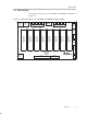
User's Guide Power Amplifier TAS5508-5121K8EVM


Digital Audio Interface (J40)
2-7
System Interfaces
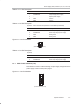
2.8 Digital Audio Interface (J40)
The digital audio interface contains digital audio signal data (I
2
S), clocks, etc.
See the TAS5508B Data Manual (SLES162) for signal timing and details not
explained in this document.
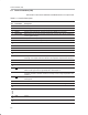
Table 2−12.J40 Pin Description
Pin
No.
Net-Name at
Schematics
Description
1 GND Ground
2 MCLK Master clock input. Low-jitter system clock for PWM generation and reclocking.
Ground connection from source to the TAS5508B must be a low-impedance
connection.
3 GND Ground
4 SDIN1 I
2
S data 1, channel 1 and 2
5 SDIN2 I
2
S data 2, channel 3 and 4
6 SDIN3 I
2
S data 3, channel 5 and 6
7 SDIN4 I
2
S data 4, channel 7 and 8
8 Reserved
9 Reserved
10 GND Ground
11 SCLK I
2
S bit clock
12 GND Ground
13 LRCLK I
2
S left−right clock
14 GND Ground
15 Reserved
16 GND Ground