
Incor User's Guide Digital Amplifier TAS5518

www.ti.com
2.1 Power Supply (PSU) Interface (J901 and J900)
Output-StagePowerSupply
SystemPowerSupply
RESET
>1ms
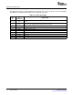
4
1
2
3
PCBConnector
(TopView)
Power Supply (PSU) Interface (J901 and J900)
The TAS5518-5152K8EVM module must be powered from external power supplies. High-end audio
performance requires a stabilized power supply, with low ripple voltage and low output impedance.
Note: The length of power-supply cable must be minimized. Increasing the length of PSU cable
is equal to increasing the distortion for the amplifier at high output levels and low
frequencies.
Maximum output-stage supply voltage depends of the speaker load resistance. Check the recommended
maximum supply voltage in the TAS5152 data sheet.
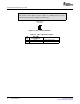
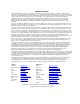
Table 2-1. Recommended Supply Voltages
VOLTAGE LIMITATIONS CURRENT
DESCRIPTION
(4- Ω LOAD) RECOMMENDATIONS
System power supply 15 V to 20 V 0.3 A
Output-stage power supply 0 V to 35 V 6 A
(1)
(1)
The rated current corresponds to two-channel full scale (80 W each), which is adequate for a
standard eight-channel amplifier design.
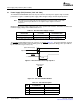
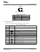
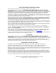
The recommended TAS5152 power-up sequence is shown in Figure 2-1 . For proper TAS5152 operation,
the RESET signal should be kept low during power up. RESET is pulled low during power up for 200 ms
by the onboard reset generator (U73).
Figure 2-1. Recommended Power-Up Sequence
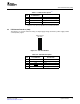
Figure 2-2. J901 and J900 Pin Numbers
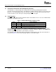
Table 2-2. J901 Pin Description
PIN NET NAME
DESCRIPTION
NO. AT SCHEMATICS
1 PVDD Output-stage power supply
2 SYSTEM System power supply
3 GND Ground
4 GND Ground
System Interfaces12 SLEU074 – June 2006
Submit Documentation Feedback