
Datasheet

TAS5614LA
SLAS846 –MAY 2012
www.ti.com
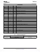
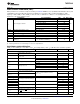
ELECTRICAL CHARACTERISTICS (continued)
PVDD_X = 36 V, GVDD_X = 12 V, VDD = 12 V, T
C
(Case temperature) = 75°C, f
S
= 384 kHz, unless otherwise specified.
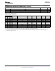
PARAMETER TEST CONDITIONS MIN TYP MAX UNIT
OTE-OTW
differential
(1)
OTE-OTW differential 30 °C
A device reset is needed to clear
OTE
HYST
(1)
25 °C
FAULT after an OTE event
OLPC Overload protection counter f
PWM
= 384 kHz 2.6 ms
Resistor – programmable, nominal peak current in
I
OC
Overcurrent limit protection 15 A
1Ω load, ROC = 24 kΩ
Resistor – programmable, nominal peak current in
I
OC_LATCHED
Overcurrent limit protection, latched 15 A
1Ω load, ROC = 62 kΩ
Time from application of short condition to Hi-Z of
I
OCT
Overcurrent response time 150 ns
affected half bridge
Internal pulldown resistor at output of Connected when RESET is active to provide
I
PD
3 mA
each half bridge bootstrap charge. Not used in SE mode.
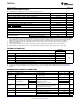
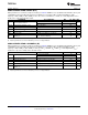
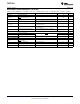
STATIC DIGITAL SPECIFICATIONS
V
IH
High level input voltage 1.9 V
INPUT_X, M1, M2, M3, RESET
V
IL
Low level input voltage 0.8 V
LEAKAGE Input leakage current 100 μA
OTW / SHUTDOWN (FAULT)
Internal pullup resistance, OTW, CLIP,
R
INT_PU
20 26 33 kΩ
FAULT to DVDD
V
OH
High level output voltage Internal pullup resistor 3 3.3 3.6 V
V
OL
Low level output voltage I
O
= 4mA 200 500 mV
FANOUT Device fanout OTW, FAULT, CLIP No external pullup 30 devices
10 Submit Documentation Feedback Copyright © 2012, Texas Instruments Incorporated
Product Folder Link(s): TAS5614LA