
Datasheet

TAS5614LA
SLAS846 –MAY 2012
www.ti.com
THEORY OF OPERATION
POWER SUPPLIES
To facilitate system design, the TAS5614LA needs only a 12V supply in addition to the (typical) 36 V power-
stage supply. An internal voltage regulator provides suitable voltage levels for the digital and low-voltage analog
circuitry. Additionally, all circuitry requiring a floating voltage supply, e.g., the high-side gate drive, is
accommodated by built-in bootstrap circuitry requiring only an external capacitor for each half-bridge.
To provide outstanding electrical and acoustical characteristics, the PWM signal path including gate drive and
output stage is designed as identical, independent half-bridges. For this reason, each half-bridge has separate
bootstrap pins (BST_X) and each full-bridge has separate power stage supply (PVDD_X) and gate supply
(GVDD_X) pins. Furthermore, an additional pin (VDD) is provided as supply for all common circuits. Although
supplied from the same 12 V source, it is highly recommended to separate GVDD_AB, GVDD_CD, and VDD on
the printed-circuit board (PCB) by RC filters (see application diagram for details). These RC filters provide the
recommended high-frequency isolation. Special attention should be paid to placing all decoupling capacitors as
close to their associated pins as possible. In general, inductance between the power supply pins and decoupling
capacitors must be avoided. (See reference board documentation for additional information.)
Special attention should be paid to the power-stage power supply; this includes component selection, PCB
placement, and routing. As indicated, each full-bridge has independent power-stage supply pins (PVDD_X). For
optimal electrical performance, EMI compliance, and system reliability, it is important that each PVDD_X
connection is decoupled with minimum 2x 220 nF ceramic capacitors placed as close as possible to each supply
pin. It is recommended to follow the PCB layout of the TAS5614LA reference design. For additional information
on recommended power supply and required components, see the application diagrams in this data sheet.
The 12V supply should be from a low-noise, low-output-impedance voltage regulator. Likewise, the 36 V power-
stage supply is assumed to have low output impedance and low noise. The power-supply sequence is not critical
as facilitated by the internal power-on-reset circuit. Moreover, the TAS5614LA is fully protected against
erroneous power-stage turn on due to parasitic gate charging when power supplies are applied. Thus, voltage-
supply ramp rates (dV/dt) are non-critical within the specified range (see the Recommended Operating
Conditions table of this data sheet).
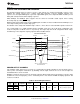
Boot Strap Supply
For a properly functioning bootstrap circuit, a small ceramic capacitor must be connected from each bootstrap pin
(BST_X) to the power-stage output pin (OUT_X). When the power-stage output is low, the bootstrap capacitor is
charged through an internal diode connected between the gate-drive power-supply pin (GVDD_X) and the
bootstrap pin. When the power-stage output is high, the bootstrap capacitor potential is shifted above the output
potential and thus provides a suitable voltage supply for the high-side gate driver. In an application with PWM
switching frequencies in the range from 300kHz to 400 kHz, it is recommended to use 33 nF ceramic capacitors,
size 0603 or 0805, for the bootstrap supply. These 33-nF capacitors ensure sufficient energy storage, even
during minimal PWM duty cycles, to keep the high-side power stage FET (LDMOS) fully turned on during the
remaining part of the PWM cycle.
SYSTEM POWER-UP/POWER-DOWN SEQUENCE
Powering Up
The TAS5614LA does not require a power-up sequence. The outputs of the H-bridges remain in a high-
impedance state until the gate-drive supply voltage (GVDD_X) and VDD voltage are above the undervoltage
protection (UVP) voltage threshold (see the Electrical Characteristics table of this data sheet). Although not
specifically required, it is recommended to hold RESET in a low state while powering up the device. This allows
an internal circuit to charge the external bootstrap capacitors by enabling a weak pulldown of the half-bridge
output.
Powering Down
The TAS5614LA does not require a power-down sequence. The device remains fully operational as long as the
gate-drive supply (GVDD_X) voltage and VDD voltage are above the undervoltage protection (UVP) voltage
threshold (see the Electrical Characteristics table of this data sheet). Although not specifically required, it is a
good practice to hold RESET low during power down, thus preventing audible artifacts including pops or clicks.
14 Submit Documentation Feedback Copyright © 2012, Texas Instruments Incorporated
Product Folder Link(s): TAS5614LA