
Datasheet

/RESET
OUT_X
3.3V
0V
Hi-Z
DC_RAMP
PVDD_X
0V
SPEAKER OUT_X
STARTUP/SHUTDOWN RAMP
VI_CM
0V
50%
PVDD_X/2
0V
Ramp Start Ramp End Ramp Start Ramp End
OUT_X IS SWITCHING (MUTE)
OUT_X IS SWITCHING (MUTE)
INPUT_X Hi-Z
3. 3V
0V
INPUT_X IS SWITCHING (MUTE)
NOISE SHAPER OFF
INPUT_X IS SWITCHING (MUTE)
NOISE SHAPER OFF
t
Startup Ramp
t
Startup Ramp
(UNMUTED)
(UNMUTED)
INPUT_X IS SWITCHING (MUTE)
NOISE SHAPER ON
TAS5614LA
www.ti.com
SLAS846 –MAY 2012
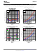
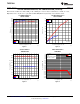
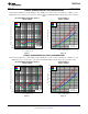
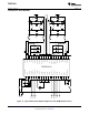
STARTUP AND SHUTDOWN RAMP SEQUENCE
The integrated startup and stop sequence ensures a click and pop free startup and shutdown sequence of the
amplifier. The startup sequence uses a voltage ramp with a duration set by the CSTART capacitor. The
sequence uses the input PWM signals to generate output PWM signals, hence input idle PWM should be present
during both startup and shut down ramping sequences.
VDD, GVDD_X and PVDD_X power supplies must be turned on and with settled outputs before starting
the startup ramp by setting RESET high.
During startup and shutdown ramp the input PWM signals should be in muted condition with the PWM processor
noise shaper activity turned off (50% duty cycle).
The duration of the startup and shutdown ramp is 100 ms + X ms, where X is the CSTART capacitor value in nF.
It is recommended to use 100nF CSTART in BTL and PBTL mode and 1 µF in SE mode configuration. This
results in ramp times of 200 ms and 1.1s respectively. The longer ramp time in SE configuration allows charge
and discharge of the output AC coupling capacitor without audible artifacts.
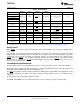
UNUSED OUTPUT CHANNELS
If all available output channels are not used, it is recommended to disable switching of unused output nodes to
reduce power consumption. Furthermore by disabling unused output channels the cost of unused output LC
demodulation filters can be avoided.
Disabling a channel is done by leave the bootstrap capacitor (BST) unstuffed and connecting the respective input
to GND. The unused output pin(s) can be left floating. Please note that the PVDD decoupling capacitors still
need to be mounted.
Table 2. Unused Output Channels
Operating PWM Output Unused
INPUT_A INPUT_B INPUT_C INPUT_D Unstuffed Component
Mode Input Configuration Channel
000 2N + 1
AB GND GND PWMc PWMd BST_A & BST_B capacitor
001 1N + 1 2 x BTL
CD PWMa PWMb GND GND BST_C & BST_D capacitor
010 2N + 1
Copyright © 2012, Texas Instruments Incorporated Submit Documentation Feedback 15
Product Folder Link(s): TAS5614LA