
Datasheet

TAS5614LA
SLAS846 –MAY 2012
www.ti.com
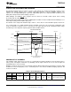
Table 5. Fault Handling
Fault/Event Global or
Reporting Latched/Self
Fault/Event Action needed to Clear Output FETs
Method Clearing
Description Channel
PVDD_X UVP
VDD UVP
Increase affected supply
Voltage Fault Global FAULT Pin Self Clearing Hi-Z
voltage
GVDD_X UVP
AVDD UVP
Power On
POR (DVDD UVP) Global FAULT Pin Self Clearing Allow DVDD to rise H-Z
Reset
Allow BST cap to recharge
Channel (half
BST UVP Voltage Fault None Self Clearing HighSide Off
bridge)
(low side on, VDD 12V)
Thermal Cool below lower OTW
OTW Global OTW Pin Self Clearing Normal operation
Warning threshold
Thermal
OTE (OTSD) Global FAULT Pin Latched Toggle RESET Hi-Z
Shutdown
OLP (CBC >2.6ms) OC shutdown Channel FAULT Pin Latched Toggle RESET Hi-Z
Latched OC (ROC >47k) OC shutdown Channel FAULT Pin Latched Toggle RESET Hi-Z
reduce signal level or Flip state, cycle by
CBC (24k<ROC<33k) OC Limiting Channel None Self Clearing
remove short cycle at fs/2
Stuck at Fault
(1)
(1 to 3
No PWM Channel None Self Clearing resume PWM Hi-Z
channels)
Stuck at Fault
(2)
(All
No PWM Global None Self Clearing resume PWM Hi-Z
channels)
(1) Stuck at Fault occurs when input PWM drops below minimum PWM frame rate given in Recommended Operating Conditions.
(2) Stuck at Fault occurs when input PWM drops below minimum PWM frame rate given in Recommended Operating Conditions.
DEVICE RESET
When RESET is asserted low, all power-stage FETs in the four half-bridges are forced into a high-impedance
(Hi-Z) state.
In BTL modes, to accommodate bootstrap charging prior to switching start, asserting the reset input low enables
weak pulldown of the half-bridge outputs. In the SE mode, the output is forced into a high impedance state when
asserting the reset input low. Asserting reset input low removes any fault information to be signaled on the
FAULT output, i.e., FAULT is forced high. A rising-edge transition on reset input allows the device to resume
operation after an overload fault. To ensure thermal reliability, the rising edge of RESET must occur no sooner
than 4 ms after the falling edge of FAULT.
SYSTEM DESIGN CONSIDERATION
A rising-edge transition on reset input allows the device to execute the startup sequence and starts switching.
Apply audio only according to the timing information for startup and shutdown sequence. That will start and stop
the amplifier without audible artifacts in the output transducers.
The CLIP signal indicates that the output is approaching clipping (when output PWM starts skipping pulses due
to loop filter saturation). The signal can be used to initiate an audio volume decrease or to adjust the power
supply rail.
The device inverts the audio signal from input to output.
The DVDD and AVDD pins are not recommended to be used as a voltage source for external circuitry.
18 Submit Documentation Feedback Copyright © 2012, Texas Instruments Incorporated
Product Folder Link(s): TAS5614LA