
Datasheet
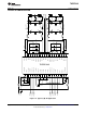


T1
T2
T3
T5
T5
T6
TAS5614LA
SLAS846 –MAY 2012
www.ti.com
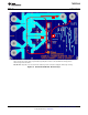
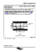
PCB copper must be at least 1 ounce thickness. PVDD and output traces must be wide enough to carry
expected average currents without excessive temperature rise. PWM input traces must be kept short and close
together on the input side of the IC and must be shielded with ground flood to avoid interference from high power
switching signals.
The heatsink must be grounded well to the PCB near the IC, and a thin layer of highly conductive thermal
compound (about 1mil) must be used to connect the heatsink to the PowerPAD.
Note T1: Bottom and top layer ground plane areas are used to provide strong ground connections. The area under
the IC must be treated as central ground, with IC grounds connected there and a strong via matrix connecting the
area to bottom ground plane. The ground path from the IC to the power supply ground through top and bottom layers
must be strong to provide very low impedance to high power and audio currents.
Note T2: Low impedance X7R or X5R ceramic high frequency decoupling capacitors must be placed within 2mm of
PVDD and GND pins and connected directly to them and to top ground plane to provide good decoupling of high
frequency currents for best performance and reliability. Their DC voltage rating must be 2 times PVDD.
Note T3: Low impedance electrolytic bulk decoupling capacitors must be placed as close as possible to the IC.
Typically the heat sink sets the distance. Wide PVDD traces are routed on the top layer with direct connections to the
pins, without going through vias.
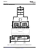
Note T4: LC filter inductors and capacitors must be placed as close as possible to the IC after decoupling capacitors.
Inductors must have low DC resistance and switching losses and must be linear to at least the OCP (over current
protection) limit. Capacitors must be linear to at least twice the maximum output voltage and must be capable of
conducting currents generated by the maximum expected high frequency output.
Note T5: Bulk decoupling capacitors and LC filter capacitors must have strong ground return paths through ground
plane to the central ground area under the IC.
Note T6: The heatsink must have a good thermal and electrical connection to PCB ground and to the IC PowerPAD.
It must be connected to the PowerPAD through a thin layer, about 1 mil, of highly conductive thermal compound.
Figure 16. Printed Circuit Board - Top Layer
24 Submit Documentation Feedback Copyright © 2012, Texas Instruments Incorporated
Product Folder Link(s): TAS5614LA